GaAs Wafers for Photo-Emission Spectroscopy
A PhD in physics requested a quote for the following.
I am interested in a GaAs wafer. My application is not a device, I need it
for an ARPES experiment. It will be cut in small pieces and cleaved in
vacuum so the orientation is not important. Could you offer some cheap wafer
of GaAs?
Question:
And what does undoped SI GaAs:-, is it GaAs film on Si wafer? Again sorry for the questions, I am not a nano-engineer!
Answer:
"Undoped SI GaAs:-" means "undoped Semi-Insulating Gallium Arsenide".
This means that the material is ultra-pure and no dopant was added, and the material was processed so as to be Semi-Insulating, that its resistivity is higher than ten million Ohm cm. It is monocrystalline GaAs.
In Semi-Insulating material, there will be very few electrons in the valance band, Charge Carrier density of the order of 1E8 charge carriers per cubic centimeter of GaAs {for item #5451, it is listed as 2.1E7 a/cc}. I am uncertain if that will help or hinder your ARPES experiments.
Other undoped GaAs, like item #5481 has Nc=3.45E15/cc. That is no longer considered Semi-Insulating.
Semi-Conductive GaAs, in case of #K501, expresly doped with Tellurium, has n-type Nc=1.9E18/cc. Now you have very many charge carriers in the valance band.
Fortunately perhaps, what we offered is monocrystalline GaAs a wide range of resistivities, for you to choose from. I know too little about "Angle-resolved photo-emission spectroscopy" to advise you what to use.
Note also that 1E8 means 1 time ten to the eighth power, and similarly for the other numbers expressed in the "E" convention.
Get Your Silicon Wafer Quote FAST! Or, Buy Online and Start Researching Today!
Carriers for Secondary Ion Emission Spectroscopy
A postdoc requested a quote for the following.
Question:
I'd like to order a pack of n-
type pure Si wafers. The
diameter needed is 1 inch.
What should be the price and
the procedure?
The only specifications required are: chemical composition Si with no impurities diameter 1 inch or slightly less (~2.3 cm)
n-type.
Maybe you can recommend which one is better as a substrate for secondary mass spectroscopy?
Answer:
As substrates or sample carriers for Secondary Ion Emission Spectroscopy, you want the purest Silicon that you can get. That means Float Zone (FZ) crystallized Silicon with the highest resistivity available. I recommend #K148 or L148. You can purchase these in a sealed cassette of 25 or 23 or 21 wafers.
Actually G519 would be just as good. I do not recommend CZ crystallized Silicon wafers like #3656 because they contain about 20ppma of Oxygen and about 1ppma of Carbon, but if these elements do not affect you then they are almost as good but less expensive.
Reference #209170 for specs and pricing.
What is Emission Spectroscopy?
mission spectroscopy is a technique used to study the light emitted by atoms, molecules, or ions when  they return to a lower energy state from an excited state. The process involves the following steps:
-
Excitation: The sample is excited using an external energy source such as heat (flame), electric discharge, or a laser. This excitation provides enough energy to move electrons in the atoms or molecules to higher energy levels.
-
Emission: When the electrons return to their original, lower energy levels, they emit light at specific wavelengths. This emitted light is characteristic of the element or compound and can be analyzed to determine its composition.
-
Detection: The emitted light is collected and passed through a spectrometer, which disperses the light into its component wavelengths. The resulting spectrum can be recorded and analyzed.
The spectrum obtained in emission spectroscopy consists of lines or bands at specific wavelengths corresponding to the energy differences between the excited and ground states of the electrons. Each element has a unique emission spectrum, which acts like a fingerprint, allowing for the identification and quantification of elements in a sample.
Applications of Emission Spectroscopy
- Chemical Analysis: Identifying and quantifying elements in various samples, such as metals, minerals, and biological tissues.
- Astronomy: Determining the composition of stars and other celestial bodies.
- Environmental Monitoring: Detecting pollutants and heavy metals in air, water, and soil.
- Industrial Applications: Quality control and process monitoring in manufacturing and metallurgy.
Common types of emission spectroscopy include flame emission spectroscopy (FES), atomic emission spectroscopy (AES), and inductively coupled plasma emission spectroscopy (ICP-OES).
What Are Commonly Used Substrate Specs for Emission Spectroscopy?
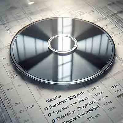
The specifications of a substrate can vary widely depending on the specific application and the materials being used. However, in semiconductor manufacturing, silicon wafers are the most commonly used substrates. Here are the typical specifications for silicon wafers:
- Common Sizes: 100 mm (4 inches), 150 mm (6 inches), 200 mm (8 inches), and 300 mm (12 inches)
- Most Common: 200 mm and 300 mm are widely used in modern semiconductor fabrication.
Type
- Monocrystalline Silicon: Most common for high-quality semiconductor devices.
Dopant
- Common Dopants:
- Boron (p-type): For creating positive charge carriers.
- Phosphorus (n-type): For creating negative charge carriers.
- Arsenic (n-type): Also used for creating negative charge carriers, especially in high-concentration doping.
Orientation
- Common Orientations:
- <100>: Most widely used orientation for silicon wafers due to its favorable electronic properties.
- <111>: Used for specific applications requiring different electronic characteristics or mechanical properties.
- <110>: Less common but used in certain niche applications.
Resistivity
- Range:
- Low Resistivity (0.001 to 0.1 ohm-cm): Highly doped wafers for certain applications like power devices.
- High Resistivity (1 to 1000 ohm-cm): Lightly doped wafers for high-purity applications such as MEMS (Micro-Electro-Mechanical Systems) and RF (Radio Frequency) devices.
- Typical Value: Depends on the application but common ranges are 1 to 10 ohm-cm for general semiconductor device fabrication.
Wafer Thickness
- Common Thicknesses:
- 200 mm Wafer: Typically around 725 µm.
- 300 mm Wafer: Typically around 775 µm.
- Thickness can vary slightly based on specific processing needs and wafer handling requirements.
Polish
- Single Side Polished (SSP): Most common, with one side polished to a mirror-like finish for device fabrication.
- Double Side Polished (DSP): Used for applications requiring high flatness and minimal warp, such as SOI (Silicon-On-Insulator) wafers and certain high-precision optical devices.
These specifications ensure that the silicon wafers meet the rigorous requirements for semiconductor device fabrication, including the need for high purity, precise doping, and specific mechanical and electronic properties.

 they return to a lower energy state from an excited state. The process involves the following steps: