
Custom Silicon Wafer Processing Services
UniversityWafer, Inc. provides custom silicon wafer processing services for universities, research laboratories, semiconductor manufacturers, start-ups, and prototype development projects. We can help source and process wafers to meet specific requirements for diameter, thickness, crystal orientation, resistivity, dopant type, surface finish, coatings, and device fabrication.
From wafer preparation and polishing to oxidation, thin-film deposition, dicing, and packaging, our team can support both early-stage research and production-scale processing.
Available Wafer Processing Options
- Single-Side and Double-Side Polishing: SSP and DSP wafers for lithography, bonding, optics, MEMS, and thin-film deposition.
- Thermal Oxide Growth: Custom thermal oxide wafers with specified oxide thicknesses for insulation, masking, passivation, and device fabrication.
- Silicon Nitride Deposition: Silicon nitride coatings for masking, membrane fabrication, passivation, and dielectric applications.
- TEOS and CVD Coatings: TEOS oxide and other deposited films for research, microfabrication, and semiconductor processing.
- Wafer Dicing and Scribing: Full wafers can be cut into custom dies, chips, strips, coupons, or smaller substrate pieces.
- Grinding and Wafer Thinning: Custom thickness reduction for sensors, flexible devices, MEMS structures, and advanced packaging.
- Prime, Test, and Mechanical Grades: Select the appropriate wafer grade based on surface quality, flatness, defect requirements, and budget.
- Custom Doping and Resistivity: P-type and n-type silicon with boron, phosphorus, arsenic, or antimony doping.
- Custom Crystal Orientations: Common orientations include <100>, <111>, and <110> for device fabrication and research.
- Research and Prototype Quantities: Small quantities are available for proof-of-concept testing, university research, and process development.
Applications We Support
Processed silicon wafers are available for MEMS, photonics, microelectronics, sensors, power devices, solar cells, wafer bonding, microfluidics, and semiconductor research. We can help identify suitable silicon wafer specifications based on your fabrication process and performance requirements.
Request a Custom Wafer Quote
To receive an accurate quote, include your preferred wafer diameter, thickness, orientation, dopant, resistivity, polish type, coating thickness, quantity, and any required processing tolerances.
Get Your Silicon Wafer Processing Quote FAST! Or, Buy Online and Start Researching Today!
How Are Silicon Wafers Processed?
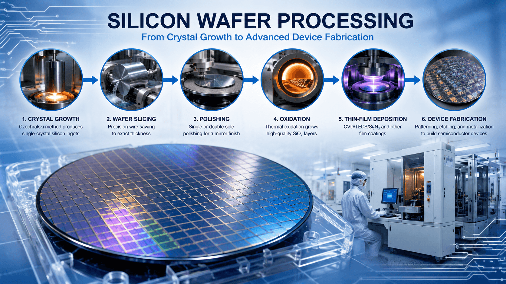
Silicon wafer processing transforms raw single-crystal silicon into flat, clean, polished substrates used for semiconductor fabrication, MEMS, sensors, photonics, solar cells, and university research. Each processing step improves the wafer’s surface quality, thickness control, cleanliness, and electrical performance before it is used to build microelectronic devices.
Silicon Crystal Growth
Most silicon wafers begin as a single-crystal silicon ingot grown by the Czochralski method. During this process, a silicon seed crystal is pulled from molten silicon to form a cylindrical ingot with a controlled crystal orientation such as <100>, <111>, or <110>. Dopants such as boron, phosphorus, arsenic, or antimony may be added to create p-type or n-type silicon with a specific resistivity range.
Wafer Slicing and Shaping
After crystal growth, the silicon ingot is sliced into thin wafers using precision diamond wire saws. The wafers are then edge-rounded, flattened, and inspected to meet diameter, thickness, bow, warp, and total thickness variation requirements. Common wafer diameters include 25mm, 50mm, 75mm, 100mm, 150mm, 200mm, and 300mm. Researchers can also request custom silicon wafer sizes and thickness specifications for specialized applications.
Lapping, Etching, and Cleaning
Lapping removes saw damage and improves wafer flatness. Chemical etching is then used to remove subsurface damage and prepare the wafer for polishing. Wafer cleaning steps remove particles, metals, organic residue, and other contaminants that can affect semiconductor device performance.
Wafer Polishing
Silicon wafers can be single-side polished, double-side polished, or chemical-mechanical polished depending on the application. Prime-grade and test-grade wafers often require a smooth, low-defect surface for photolithography, thin-film deposition, oxidation, wafer bonding, and device fabrication. The appropriate polish type depends on the required surface roughness, flatness, cleanliness, and optical quality.
Oxidation, Deposition, and Etching
Additional wafer processing may include thermal oxide growth, silicon nitride deposition, TEOS oxide, metal-film deposition, photoresist coating, dry etching, wet etching, and other custom thin-film processes. These steps allow researchers and device manufacturers to create insulating layers, masks, electrical contacts, and patterned structures on the silicon surface.
Silicon Epitaxy and SOI Wafer Processing
Specialized processing can also include silicon epitaxy, in which a controlled crystalline silicon layer is grown on a silicon substrate. Researchers developing advanced transistors, photonic devices, sensors, and MEMS structures may also require silicon-on-insulator wafers with a specified device layer, buried oxide layer, and handle wafer.
Silicon Wafers for Research and Device Fabrication
Processed silicon wafers are used in integrated circuits, MEMS devices, microfluidics, sensors, photovoltaics, power electronics, optical coatings, wafer bonding, and university research projects. Choosing the correct wafer processing specification helps improve process repeatability, device yield, and experimental performance.
UniversityWafer, Inc. supplies processed silicon wafers in custom diameters, crystal orientations, thicknesses, resistivity ranges, oxide thicknesses, polish types, and dopant types for research and production.