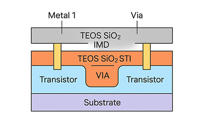
What is TEOS tetraethyl orthosilicate and why is it important for fabricating semiconductors?

Tetraethyl orthosilicate (TEOS) is a silicon-containing chemical compound used extensively in semiconductor manufacturing to create high-quality silicon dioxide (SiO₂) thin films.
-
Chemical formula: Si(OC₂H₅)₄
-
Type: Silicon alkoxide precursor
-
State: Clear liquid at room temperature
-
Common use: Precursor for depositing silicon dioxide films
In simple terms, TEOS is a liquid source of silicon and oxygen that can be converted into SiO₂, the same material used for insulating layers on silicon wafers.
Why TEOS Is Important in Semiconductor Fabrication
1. Depositing Silicon Dioxide Films
TEOS is widely used to deposit SiO₂ dielectric layers in microelectronics.
When TEOS decomposes in a reactor (usually by heat or plasma), it forms:
Si(OC2H5)4+O2→SiO2+CO2+H2OSi(OC_2H_5)_4 + O_2 \rightarrow SiO_2 + CO_2 + H_2OThis reaction leaves behind a thin film of silicon dioxide on the wafer surface.
Why this matters
Silicon dioxide is one of the most important materials in semiconductor devices because it acts as:
-
Electrical insulation
-
Gate oxide in transistors
-
Interlayer dielectric
-
Surface passivation
-
Isolation between metal layers
Where TEOS Is Used in Semiconductor Processing
1. Chemical Vapor Deposition (CVD)
TEOS is most commonly used in CVD processes:
LPCVD (Low Pressure CVD)
-
Temperature: 650–750°C
-
Produces high-quality conformal oxide
PECVD (Plasma Enhanced CVD)
-
Temperature: 300–400°C
-
Used when wafers cannot tolerate high heat
Sub-Atmospheric CVD (SACVD)
-
Used for interlayer dielectric gap fill
Key Advantages of TEOS Oxide
1. Excellent Conformal Coverage
TEOS oxide coats complex topography very well.
This is critical for modern devices with:
-
trenches
-
vias
-
high-aspect-ratio features
2. High Film Uniformity
TEOS processes produce oxide films with:
-
good thickness uniformity
-
smooth surfaces
-
controlled density
3. Good Step Coverage
Unlike some oxide deposition methods, TEOS can cover:
-
vertical sidewalls
-
narrow trenches
-
deep vias
This is essential in multilevel metal interconnects.
4. Lower Particle Contamination
Because TEOS is a clean liquid precursor, it often produces fewer particles compared with some silane-based processes.
TEOS vs Silane Oxide Deposition
| Property | TEOS Oxide | Silane Oxide |
|---|---|---|
| Source | Liquid precursor | Gas precursor |
| Conformality | Excellent | Moderate |
| Deposition temperature | Medium–High | Lower |
| Film density | High | Lower |
| Gap fill | Very good | Moderate |
For many advanced IC processes, TEOS oxide is preferred.
Other Uses of TEOS
Beyond semiconductor fabs, TEOS is used in:
-
Sol-gel processes
-
Optical coatings
-
Aerogels
-
Silica nanoparticles
-
MEMS devices
-
Anti-reflection coatings
Given your work with wafer substrates, thin films, and MEMS fabrication, TEOS oxide is probably encountered frequently in LPCVD or PECVD dielectric layers deposited on silicon wafers.
Interesting industry fact:
For decades, TEOS oxide has been the workhorse interlayer dielectric in CMOS processes, especially in nodes from about 1 µm down to ~90 nm before newer low-k dielectrics began replacing it in advanced interconnect stacks.

