Can you supply sapphire wafers with AlGaN coating?
Required dimensions were approximately 1 cm diameter or larger with substrate thicknesses between 200 and 500 µm.
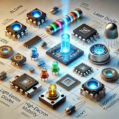
Aluminum Gallium Nitride (AlGaN) wafers and AlGaN/GaN heterostructures are widely used in UV LEDs, laser diodes, HEMTs, RF electronics, and wide-bandgap semiconductor research. UniversityWafer supplies AlGaN on sapphire templates and custom epitaxial structures for optoelectronic devices, high-power transistors, and deep-ultraviolet applications.

Aluminum Gallium Nitride (AlGaN) is a wide-bandgap semiconductor material widely used for UV LEDs, laser diodes, high-power electronics, photodetectors, and deep ultraviolet light sources. AlGaN epitaxial layers grown on sapphire substrates offer excellent thermal stability, optical properties, and compatibility with GaN device fabrication.
A senior consulting scientist requested AlGaN-coated sapphire wafers for lamp, laser and LED research.
Can you supply sapphire wafers with AlGaN coating?
Required dimensions were approximately 1 cm diameter or larger with substrate thicknesses between 200 and 500 µm.
UniversityWafer, Inc. quoted:
Reference #164039 for pricing and specifications.
AlGaN templates and AlGaN/GaN heterostructures are commonly used in:
Get Your AlGaN Quote FAST! Or, Buy Online and start researching today.
Undoped c-plane AlGaN templates are frequently used for epitaxial growth studies, UV emitters, and semiconductor device characterization. Low defect densities and smooth surfaces are critical for maximizing optical and electrical performance.
A graduate student requested:
2-inch diameter undoped c-plane AlGaN templates with approximately 50% aluminum composition. Required information included:
Reference #194822 for pricing and specifications.
AlGaN alloys possess large bandgaps, high breakdown fields, and excellent thermal stability, making them ideal for next-generation electronic and optoelectronic devices. Their ability to emit ultraviolet light and support high-power operation makes AlGaN one of the most important materials for advanced semiconductor technologies.
 Aluminum Gallium Nitride (AlGaN) and AlGaN/GaN heterostructures are widely used in high-frequency electronics, UV LEDs, laser diodes, HFETs, HEMTs and GaN-based transistor research. These epitaxial layers are commonly grown by MOVPE on sapphire, silicon carbide or high-resistivity silicon substrates.
A PhD candidate requested wafers for transferring HFET technology based on AlGaN/GaN heterostructures deposited on Al₂O₃ sapphire.
The customer required a semi-insulating substrate to reduce unwanted electrical influence during high-field and high-frequency transistor operation.
Reference #171068 for specifications and pricing.
P-type AlGaN templates and p-type GaN templates are used in optoelectronic devices, UV emitters, laser diodes, LEDs and advanced semiconductor research. Magnesium-doped GaN and AlGaN layers can be deposited on sapphire or quartz substrates depending on the application requirements.
A postdoctoral researcher requested p-type GaN and p-type AlGaN templates with detailed electrical, optical, mechanical and surface data. Desired film thickness was approximately 0.3–0.8 µm on sapphire or quartz, with substrate stability above 1000°C.
Reference #197858 for specifications and pricing.
Research-grade AlGaN templates are available with different aluminum compositions, dopants, buffer layers and epitaxial thicknesses. These wafers are useful for studying carrier transport, optical emission, high electron mobility transistors and wide-bandgap semiconductor devices.
A sales engineer requested 2 inch AlGaN templates on c-plane sapphire with 200–300 nm AlGaN layers doped with silicon at 3–5 × 1018 cm-3. Target aluminum compositions were 20% and 40%.
UniversityWafer, Inc. quoted the following research-grade options:
| Substrate | Diameter | Buffer Layer | Epitaxial Layer / Dopant | Thickness |
|---|---|---|---|---|
| Sapphire | 2 inch | 50 nm AlN | GaN, intrinsic | 100 nm |
| Sapphire | 2 inch | 50 nm AlN | GaN, intrinsic | 300 nm |
| Sapphire | 2 inch | 50 nm AlN | Al10%GaN, intrinsic | 300 nm |
| Sapphire | 2 inch | 50 nm AlN | Al20%GaN, n-type / Si doped | 250 nm |
| Sapphire | 2 inch | 50 nm AlN | Al40%GaN, n-type / Si doped | 250 nm |
Reference #102784 for specifications and pricing.