What Silicon Substrates Used to Grow Nanowires for Plasmonic Applications?
A Phd candiate requested a quote for their nanowire research.
I was looking to get a quote for some silicon wafers. What I’m looking for are some silicon wafers without thermal oxide and polished on both sides. Is that possible to get something like this and if so could the specifications for everything else be the same as the wafers we had ordered before? I included our previous order below.
What I’m looking for are some silicon wafers without thermal oxide and polished on both sides. Is that possible to get something like this and if so could the specifications for everything else be the same as the wafers we had ordered before?
We are using the substrates to grown Si nanowires for plasmonic applications, and we needed the double polished and no thermal oxide wafers to be able to run FTIR measurements on the growth substrate. Without the double polished, we were not getting enough transmission through, and the thermal oxide was absorbing at longer wavelengths.
Reference RFQ#198876 for specs and pricing.
What Undoped Wafers Are Used to Grow Nanowires?
A postdoc need the following for their nanowire project.
I would like a quote and lead time for a Si wafer with 10nm Au sputter coated on top.
I'm looking for a 2 inch wafer of Si, undoped should be fine. I'm not too concerned about the specifics of the Si, it's the gold overlayer that is important for my needs (we are doing VLS growth of ZnO nanowires in a tube furnace and the sputtered gold layer acts as a seed layer/catalyst). Are you also able to dice the wafer after sputtering?
Reference # 259887 for specs and pricing.
Get Your Quote FAST! Buy Online and Start Researching Today!

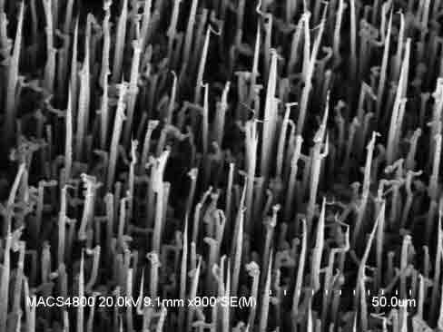
Undoped silicon nan1 Undoped Si NWs

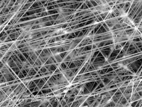
P-Doped Silicon Nanowires
What are Nanowires?
Nanowires are ultra-thin structures with a diameter on the nanoscale, typically in the range of a few nanometers to a few hundred nanometers. They are typically made of semiconducting or metallic materials, and are typically several orders of magnitude longer than they are wide.
Nanowires can be grown using a variety of methods, including chemical vapor deposition, electrochemical deposition, and molecular beam epitaxy. They have a wide range of potential applications, including in electronics, sensors, and energy conversion and storage.
In electronics, nanowires can be used to make smaller and more efficient transistors and other electronic components. In sensors, they can be used to detect and measure various physical and chemical properties, such as temperature, pressure, and gas concentrations. In energy conversion and storage, nanowires can be used in solar cells, batteries, and fuel cells to improve their efficiency and performance.
What Substrates are Used to Grow Nanowires?
Nanowires can be grown on a variety of substrates, depending on the material system and growth technique used. Some commonly used substrates for nanowire growth include:
-
Silicon: Silicon is one of the most commonly used substrates for nanowire growth, particularly for the growth of semiconductor nanowires. It is readily available and has a well-established fabrication process, which makes it a convenient substrate for nanowire growth.
-
Quartz: Quartz is another popular substrate for nanowire growth, especially for the growth of oxide-based nanowires. It is transparent, chemically inert, and has a low thermal expansion coefficient, making it well-suited for high-temperature growth processes.
-
Sapphire: Sapphire is a popular substrate for the growth of nitride-based nanowires, such as gallium nitride (GaN) and aluminum nitride (AlN). It has a high melting point and good thermal stability, which makes it suitable for high-temperature growth processes.
-
Metal films: Thin metal films, such as gold, silver, or nickel, are often used as substrates for the growth of metallic nanowires. The metal film provides a nucleation site for the nanowire growth and can be easily patterned using standard lithography techniques.
-
Other materials: Other materials, such as glass, polymers, and even biological substrates, have also been used as substrates for nanowire growth. The choice of substrate depends on the specific application and the properties of the nanowire material being grown.
UniversityWafer, Inc. offers a selection of high-purity MOCVD grown silicon nanowires for use in a variety of applications including:
These nanowires can be un-doped, P-doped or N-doped and can be delivered on Si wafers or
metal foils. Growth can be on seeded substrates or can be self seeded (see listing below).
Specialty Nanowires such as SiGe, ZnO, or CNTs can also be requested.
SMI also offers Si Nanowire deposition on SMI supplied or customer supplied substrates.
SMI also offers wafer seed layer fabrication services.
Seed Layers:
- Colloidal Au
- Self Seeded
- Thin Film evaporated Au
Typical Properties:
- Undoped
- P-Type
- N-Type
- Self Seeded
Available Substrates:
- Copper Foils
- Si Wafer
- Al2O3
1 Undoped Si NWs 2 P-Doped SiNWs
3 N-Doped

