Wafers Used to Fabricate Photoconductive Antenna
A PhD student requested help with their following project.
I want to investigate fabricating photoconductive antenna using fs fiber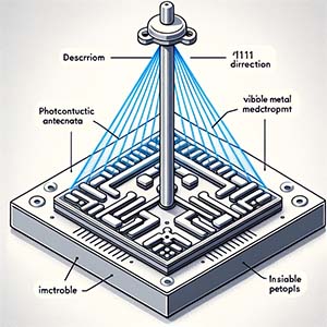 laser with wavelength of 1550 nm.
I am writing to inquire about the availability and pricing of semiconductor wafers that your esteemed company offers.
I would appreciate if you could provide me with details on:
- The range of semiconductor wafers that you offer, along with their respective specifications and applications.
- The pricing for each type of wafer.
- Any recommendations or alternatives that might suit my requirements, based on your expertise.
- Lead times for order fulfillment and delivery options.
- Information on any volume discounts or special offers that may be applicable.
While I have a general understanding of my requirements, I am open to suggestions from experts such as yourselves, and would greatly appreciate any guidance or recommendations you might offer.
Reference #278559 for specs and pricing.
Get Your Quote FAST! Or, Buy Online and Start Researching Today!
What Substrates are Used to Fabricate Photoconductive Antenna?
Photoconductive antennas (PCAs) are widely used in terahertz (THz) time-domain spectroscopy and imaging systems. They are designed to convert ultrafast optical pulses into THz electromagnetic waves and vice versa. The fabrication of a photoconductive antenna typically involves the use of specific substrates and materials that have good photoconductive properties. Here are the common substrates used for fabricating photoconductive antennas:
-
Low-Temperature-Grown (LTG) GaAs (Gallium Arsenide): One of the most popular substrates for PCA fabrication. LTG GaAs is grown at lower temperatures than normal GaAs, which results in a high concentration of crystal defects. These defects act as ultrafast recombination centers, making LTG GaAs suitable for generating and detecting THz radiation.
-
Semi-Insulating (SI) GaAs: Another form of GaAs that's often used for PCA fabrication, especially for older designs.
-
Fe-doped InGaAs (Iron-doped Indium Gallium Arsenide): This material offers faster carrier recombination times compared to undoped InGaAs, making it suitable for THz generation and detection.
-
ZnTe (Zinc Telluride): Sometimes used for THz generation and detection due to its nonlinear properties.
-
InP (Indium Phosphide): A less common substrate but still occasionally used in PCA fabrication.
-
InGaAs/InAlAs (Indium Gallium Arsenide/Indium Aluminum Arsenide) heterostructures: These are used in some advanced PCA designs due to their unique electrical properties.
A Phd Student Requested the following:
InGaAs wafer for photodetectors
Reference 248354 for our specs and pricing.
-
InSb (Indium Antimonide): Has been explored for its potential benefits in THz applications.
-
Silicon (Si): Though not as common as GaAs, silicon has been explored as a substrate for PCA due to its widespread availability and mature fabrication techniques.
In addition to these substrates, the fabrication process also involves the deposition of metal electrodes, usually made of gold (Au) or titanium (Ti), onto the substrate. The design and geometry of these electrodes play a crucial role in the performance of the PCA.
It's worth noting that the choice of substrate and its quality can significantly impact the efficiency, bandwidth, and overall performance of the photoconductive antenna. As such, ongoing research continues to explore new materials and fabrication techniques to optimize PCAs for various THz applications.
What are Photodetector Devices?
Photodetector devices are sensors of light or other electromagnetic energy. They convert incident light into an 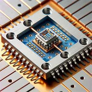 electrical signal, essentially translating photon energy into an electrical current or voltage. Photodetectors have a wide range of applications, from consumer electronics to scientific research. Here's an overview of photodetector devices:
Photodiodes: These are semiconductor devices that operate in reverse bias. When photons are absorbed, they generate electron-hole pairs. The applied reverse bias causes these carriers to flow as a current. Photodiodes are used in various applications, including solar cells, optical communication, and light metering.
Phototransistors: Similar to photodiodes, but with amplification capabilities. They have a base, collector, and emitter, and when light strikes the base, it modulates the current flow between the collector and emitter.
Photomultiplier Tubes (PMTs): These are highly sensitive detectors that can detect low levels of light. When a photon hits the photocathode inside the PMT, it releases an electron, which is then amplified as it passes through a series of dynodes, producing a cascade of electrons.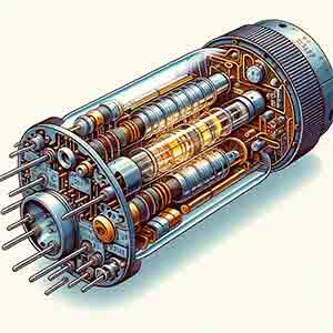
Avalanche Photodiodes (APDs): These operate under high reverse bias, close to their breakdown voltage. The high electric field accelerates photogenerated carriers, leading to the generation of secondary carriers through impact ionization. This results in internal amplification of the photocurrent.
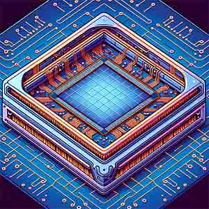 Charge-Coupled Devices (CCDs): Used primarily in imaging applications, such as digital cameras and telescopes. They collect and move charge within the device to an area where the charge can be read, effectively converting the light signal into an electrical one.
CMOS (Complementary Metal-Oxide-Semiconductor) 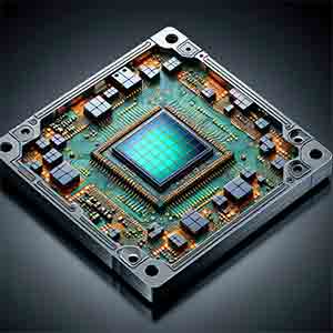 Image Sensors: Similar in function to CCDs but with a different mechanism. Each pixel in a CMOS sensor has its own charge-to-voltage conversion, and the sensor often includes amplifiers, noise-correction, and digitization circuits.
Photoresistors or Light-Dependent Resistors (LDRs): Their resistance changes based on the amount of light they receive. They are often used in light-sensing circuits and are found in devices like night lights and outdoor lighting systems  that turn on or off based on ambient light levels.
-
Pyroelectric Detectors: They respond to temperature changes caused by the absorption of light. They are often used in infrared detectors and thermal imaging.
Bolometers: These are devices that measure the power of incident electromagnetic radiation via the heating of a material with a temperature-dependent electrical resistance. They are 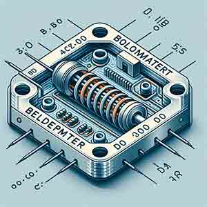 especially useful in the infrared range.
Quantum Dot Photodetectors: These utilize quantum dots, which are semiconductor nanoparticles, to absorb light and generate charge carriers.
Photodetector devices find applications in a myriad of fields, including telecommunications, medical imaging, astronomy, industrial automation, environmental sensing, and consumer electronics, among others. Their design and operation principles vary based on the specific application and the type of light they are intended to detect.
Are (111) direction substrates a suitable option for manufacturing photodetectors due to the better mobility of charge carriers?
Yes, (111) direction substrates are often considered suitable for manufacturing photodetectors due to enhanced mobility of charge carriers. The (111) orientation, in particular, is known to exhibit high electron and hole mobilities in certain semiconductor materials. (111) mproves mobility can lead to faster response times and improved sensitivity in photodetectors. However, the suitability also depends on the specific semiconductor material in use and the intended application of the photodetector. It's essential to consider other factors like epitaxial growth quality, surface recombination, and fabrication processes when choosing a substrate orientation.
What Substrates are Used to Fabricate Infrared Photodetectors?
A PhD Researcher asked for the following quote:
We are working on the infrared photodetectors and optoelectronics. What substrate can you recommend?
Reference ##ONLQ43013 for specs and pricing.
 laser with wavelength of 1550 nm.
 electrical signal, essentially translating photon energy into an electrical current or voltage. Photodetectors have a wide range of applications, from consumer electronics to scientific research. Here's an overview of photodetector devices:

 Charge-Coupled Devices (CCDs): Used primarily in imaging applications, such as digital cameras and telescopes. They collect and move charge within the device to an area where the charge can be read, effectively converting the light signal into an electrical one.
 that turn on or off based on ambient light levels.
 especially useful in the infrared range.