
We would like a few samples of GaAs that would be suitable for educational laboratory testing. The application is for photovoltaic cells. It would also be useful to have similar sets of InP .
III-V Substrates for Photovoltaic Cell Research
III-V semiconductor materials are important in advanced photovoltaic research, particularly for high-efficiency single-junction, multijunction, and concentrator photovoltaic (CPV) devices. Materials such as gallium arsenide (GaAs) and indium phosphide (InP) can be used as substrates or components of epitaxial structures for photovoltaic research.
It is important to distinguish between a semiconductor substrate and a finished photovoltaic cell. A bare GaAs or InP wafer does not by itself function as a complete solar cell. Researchers typically fabricate or grow additional semiconductor junctions, epitaxial layers, passivation layers, and electrical contacts to create a photovoltaic device.
GaAs and InP Wafers for Educational PV Research
A postdoctoral researcher requested substrate samples for an educational photovoltaic laboratory application:
Reference #110112 for specifications and pricing.
GaAs is especially important in high-performance photovoltaics because of its direct bandgap and strong optical absorption. It is used in specialized solar-cell technologies, including space photovoltaics and III-V multijunction devices. InP is also valuable in III-V photovoltaic research and can serve as a substrate for lattice-matched or engineered epitaxial semiconductor structures.
Thin Silicon Wafers for Photovoltaic Research
Crystalline silicon remains a major material platform for photovoltaic technology. Researchers developing silicon solar cells may require wafers with controlled thickness, resistivity, conductivity type, crystal orientation, and surface condition.
A solar-panel engineer requested thin silicon wafers for photovoltaic research:
Could you let us know if you have really thin silicon wafers of the type used for photovoltaic cells? The thickness would be in the range of 100 µm to 160 µm; a 5-inch diameter would be fine. We would need just a couple and would need to know the price.
Reference #145479 for specifications and pricing.
Why Wafer Thickness Matters in Photovoltaics
Reducing silicon wafer thickness can decrease semiconductor material use, but thinner wafers also become more susceptible to bowing, cracking, and breakage during handling and processing. For research applications, the appropriate thickness therefore depends on both the photovoltaic device design and the mechanical requirements of the fabrication process.
Other important specifications can include p-type or n-type conductivity, resistivity, crystal orientation, diameter, surface finish, total thickness variation, and wafer quality. The appropriate combination depends on the solar-cell architecture being investigated.
Get Your Photovoltaic Wafer Quote FAST! Or, Buy Online and Start Researching Today!
Semiconductor Materials for Concentrator Photovoltaics
Another customer requested guidance while developing concentrator photovoltaic (CPV) systems. CPV systems use optical components, such as Fresnel lenses or mirrors, to concentrate sunlight onto relatively small photovoltaic cells.
Concentrated illumination can increase the electrical output produced by a small cell area, but it also increases heat generation. Cell efficiency, thermal management, optical concentration, electrical interconnection, and device reliability therefore become important design considerations.
Our firm provides heating systems with solar panels. We are developing a new line of solar concentrators for electrical generation using photovoltaic devices and Fresnel lenses.
We are interested in high-quality photovoltaic materials that can support efficient and durable concentrator systems. Our project includes two different concentrator designs:
- Concentrator 1: A solar concentrator incorporating a liquid-cooling system, such as water or a water-glycol mixture, to control photovoltaic-cell temperature. Recovered thermal energy may potentially be used for water heating, depending on the system design.
- Concentrator 2: A solar concentrator intended for locations with limited water availability. This design would require passive cooling, air cooling, heat sinks, or another thermal-management approach that does not depend on a continuous water supply.
We are interested in technical guidance regarding semiconductor materials and photovoltaic devices suitable for these concentrator configurations.
Reference #123401 for specifications and pricing.
Why III-V Materials Are Used in Concentrator Photovoltaics
III-V semiconductors are particularly important in high-performance and concentrator photovoltaic research. Multijunction cells can combine semiconductor layers with different bandgaps so that different portions of the solar spectrum are converted more effectively than in a conventional single-junction device.
GaAs and related III-V compound semiconductors are widely studied for these applications because they can provide strong optical absorption and can be incorporated into high-efficiency epitaxial device structures. The appropriate substrate and layer structure depend on lattice matching, bandgap requirements, thermal design, optical concentration, and the intended device architecture.
Selecting Wafers for Photovoltaic Research
The best substrate depends on the photovoltaic technology being studied. Researchers working with crystalline-silicon cells may need silicon wafers with carefully controlled electrical and mechanical specifications, while III-V research may require GaAs, InP, germanium, or other substrates selected for a particular epitaxial structure.
When requesting a quote, provide the desired material, diameter, thickness, crystal orientation, conductivity type, resistivity, surface finish, quantity, and intended application when known. These specifications help identify substrate options appropriate for the photovoltaic experiment.
How Photovoltaic Cells Are Fabricated
Photovoltaic (PV) cells convert light directly into electrical energy using semiconductor materials. Crystalline silicon is the dominant material used in commercial solar cells, although thin-film semiconductors, III-V materials, perovskites, and other emerging photovoltaic materials are also used in research and specialized applications.
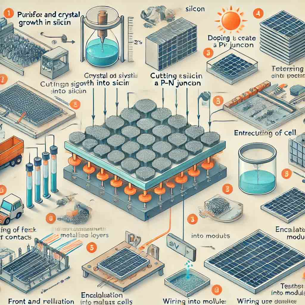
The exact fabrication sequence depends on the solar-cell architecture. For crystalline-silicon devices, manufacturing generally includes wafer preparation, surface texturing, junction or selective-contact formation, passivation, anti-reflection treatment, metallization, and electrical characterization.
1. Semiconductor and Substrate Selection
The semiconductor determines many of the electrical and optical properties of a photovoltaic device. Common photovoltaic material systems include:
- Crystalline silicon (c-Si): Used extensively for monocrystalline and multicrystalline solar cells.
- Cadmium telluride (CdTe): A thin-film photovoltaic semiconductor deposited onto a supporting substrate.
- CIGS: Copper indium gallium selenide is another thin-film absorber material.
- III-V semiconductors: Materials such as gallium arsenide (GaAs) are used in high-performance and multijunction photovoltaic devices, including specialized space applications.
- Perovskites: An actively researched class of photovoltaic absorbers that can be processed as thin films and incorporated into single-junction or tandem devices.
Substrate requirements also vary by technology. Crystalline-silicon cells use the silicon wafer itself as the semiconductor absorber, while thin-film photovoltaic devices may be fabricated on glass, metal foils, polymers, or other suitable substrates.
2. Silicon Wafer Preparation
For crystalline-silicon photovoltaics, high-purity silicon feedstock is processed into crystalline material and then formed into wafers. Monocrystalline silicon can be produced using crystal-growth methods such as the Czochralski process. The resulting ingots are shaped and sliced into thin wafers using precision wire-sawing processes.
Wafer characteristics such as crystal orientation, conductivity type, resistivity, thickness, surface condition, and impurity concentration can influence subsequent processing and device performance.
3. Surface Texturing and Cleaning
Silicon wafers can be chemically textured to reduce optical reflection and improve light trapping. On appropriately oriented monocrystalline silicon, anisotropic alkaline etching can produce microscopic pyramid structures that increase the probability that incident light enters the silicon rather than reflecting from its surface.
Cleaning steps are also important for removing particles, organic residues, metallic contamination, and unwanted surface layers before subsequent device fabrication.
4. Junction and Carrier-Selective Structure Formation
A photovoltaic device requires a structure that separates and collects photogenerated electrons and holes. In conventional crystalline-silicon cells, this can involve introducing dopants into the silicon to form regions with different conductivity types.
Boron is commonly used as a p-type dopant and phosphorus as an n-type dopant in silicon. The exact dopant arrangement depends on the cell architecture. Modern photovoltaic devices may also use passivated contacts, heterojunctions, or other carrier-selective structures rather than relying only on a simple conventional p-n junction.
5. Surface Passivation
Defects and dangling bonds at a semiconductor surface can act as recombination sites for photogenerated charge carriers. Surface passivation is therefore an important part of high-performance silicon solar-cell fabrication.
Dielectric films such as silicon nitride (SiNx), aluminum oxide (Al2O3), and silicon oxide can be incorporated into passivation schemes depending on the device design. Reducing surface recombination helps more photogenerated carriers reach the electrical contacts.
6. Anti-Reflection Coatings
An anti-reflection coating reduces the amount of incident sunlight lost by reflection from the semiconductor surface. In crystalline-silicon solar cells, silicon nitride is commonly used because it can provide both optical anti-reflection behavior and surface-passivation benefits.
Film thickness and refractive index are important parameters because the optical response of the coating depends on wavelength and interference effects.
7. Metallization and Electrical Contacts
Electrical contacts collect the charge carriers generated inside the photovoltaic device. Contact design must balance low electrical resistance with optical considerations because excessive front-side metal coverage can block incoming light.
Depending on the cell architecture and fabrication process, metal contacts may be formed using screen printing, evaporation, sputtering, electroplating, or other metallization techniques.
Modern Silicon Solar Cell Architectures
Photovoltaic research has produced several advanced crystalline-silicon architectures designed to reduce recombination and electrical losses. Examples include:
- PERC: Passivated emitter and rear cell structures use rear-surface passivation to reduce carrier recombination.
- TOPCon: Tunnel oxide passivated contact structures use thin oxide and doped silicon layers to create carrier-selective, low-recombination contacts.
- Silicon heterojunction (SHJ): Combines crystalline silicon with thin amorphous-silicon-based layers to provide passivation and carrier-selective contacts.
- Interdigitated back contact (IBC): Places electrical contacts on the rear of the device, eliminating front-contact shading.
Thin-Film Photovoltaic Cells
Thin-film solar cells are fabricated differently from conventional crystalline-silicon wafer cells. Semiconductor absorber layers are deposited onto a supporting substrate using processes that may include sputtering, evaporation, chemical vapor deposition, solution processing, or other thin-film techniques.
The complete device generally contains multiple functional layers, which may include transparent conductive oxides, electron- or hole-selective layers, semiconductor absorbers, buffer layers, and metallic contacts. Layer composition and sequence depend on the photovoltaic technology.
Perovskite and Tandem Solar Cells
Perovskite photovoltaics are an important area of solar-cell research because their optical and electronic properties can be adjusted through material composition. Perovskite absorber layers can be fabricated using solution-based or vapor-phase processes, depending on the device and research method.
Perovskites are also being investigated in perovskite-silicon tandem solar cells. In a tandem architecture, materials with different bandgaps absorb different portions of the solar spectrum, providing a route to efficiencies beyond those achievable by conventional single-junction silicon cells alone.
Photovoltaic Cell Characterization
After fabrication, photovoltaic cells can be evaluated using current-voltage (I-V) measurements under controlled illumination. Important device parameters include open-circuit voltage (VOC), short-circuit current (ISC), fill factor, and power-conversion efficiency.
Additional characterization methods can include external quantum efficiency (EQE), spectral-response measurements, reflectance measurements, photoluminescence, and other electrical, optical, and materials-analysis techniques.
From Photovoltaic Cells to Solar Modules
Cell fabrication and module manufacturing are separate stages. After individual solar cells have been fabricated and tested, cells can be electrically interconnected and encapsulated to produce a photovoltaic module.
A conventional module may incorporate front glass, encapsulant materials, interconnected solar cells, a rear protective layer or rear glass, a frame, and a junction box. These components protect the cells from environmental and mechanical stresses while allowing the module to operate outdoors.
Silicon Wafers for Photovoltaic Research
Researchers developing and characterizing photovoltaic devices may require silicon wafers with controlled diameter, thickness, crystal orientation, conductivity type, resistivity, surface finish, and other specifications. Selecting the appropriate substrate provides a controlled starting material for studying photovoltaic processing, thin films, passivation, contacts, and new solar-cell architectures.