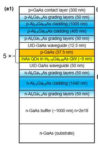
We are fabricating the QD laser and below picture is our EPI structure. We would like to purchase some Si-Gallium Arsenide (GaAs) for developing the fabrication process (used as dummy wafer). 4 inch wafer. Do you have some suggestion?
Subtrates for Quantum Dot Laser Fabrication
GaAs Wafers for QD Laser Fabrication
A postdoctoral fellow, working in a integrated photonics lab requested the following quote.

Reference #318703 for specs and pricing.
Get Your Quote FAST! Or, Buy Online and Start Researching Today!
What Substrates Are Used To Fabricate QD Lasers?
A postdoctoral research fellow requested a quote for the following.
We do research about fabricating QD laser. We want to purchase some Si doped wafer to Develop Fabrication process. Could you advise a suitable 4-inch wafer for us and sent the quotation?
Evaluating doping needs
I'm figuring out the right 4-inch silicon wafer for doping, possibly at 1e18 to 1e19 levels, for QD laser  fabrication.
Examining doping types
I'm thinking about p-type or n-type doping, which affect conductivity for ohmic contacts in QD laser fabrication. Typically, n-type doping is preferred for better conduction.
Weighing options
I'm thinking about 4-inch wafer specifications for research: <100> orientation, P or N type, 1-10 ohm-cm resistivity, 525±25 um thickness, polished surfaces, and CZ or FZ growth methods.
Choosing doping specifics
I propose a moderately doped, n-type silicon wafer at 1-10 ohm-cm, with 1e15 to 1e16 cm^-3 silicon doping, and a <100> orientation for integrated photonics.
Below is a typical set of specifications that researchers use when developing III–V/Si photonics and QD laser processes on silicon wafers. Of course, exact specs can vary depending on your specific device design and growth method, but this is a good starting point:
Recommended 4-inch (100 mm) Silicon Wafer Specifications
-
Wafer Diameter
- 100 mm (4 inch) diameter
- SEMI standard thickness of ~525 ± 25 µm
-
Crystal Orientation
- ⟨100⟩\langle 100 \rangle orientation
- This is the most commonly used orientation for epitaxy and device fabrication.
-
Type & Doping
- N-type (phosphorus or arsenic doping) is typical if you need a conductive substrate for making ohmic contacts, or for integrating with active layers that require an n-type ground plane.
- Resistivity in the range of 1–10 Ω⋅cm1 \text{–} 10~\Omega \cdot \text{cm} (which corresponds to a doping concentration of roughly 1015–1016 cm−310^{15} \text{–} 10^{16}~\text{cm}^{-3}).
- If you need a lower resistivity (more heavily doped) wafer for certain processes (e.g., to reduce substrate series resistance), you could go down to 0.001–0.01 Ω⋅cm0.001 \text{–} 0.01~\Omega\cdot\text{cm}.
- If you want more insulating behavior (to minimize leakage or crosstalk), you could go up to 10–20 Ω⋅cm10 \text{–} 20~\Omega \cdot \text{cm}.
- Float Zone (FZ) wafers are often preferred for photonics work because of their high purity and low oxygen content. However, Czochralski (CZ) wafers are more common and less expensive. If you are doing advanced epitaxy and very sensitive optical measurements, FZ might be worth the extra cost.
-
Surface Finish
- Single Side Polished (SSP) is typically sufficient if you only need to process on one side.
- Double Side Polished (DSP) can be beneficial if you need backside processing (e.g., if you intend to deposit or etch features on the backside, or require ultra-flatness).
-
Prime Grade vs. Test Grade
- Prime Grade wafers have the highest surface quality and strictest tolerance on thickness, TTV (total thickness variation), and surface defects. These are usually used for demanding device fabrication steps (e.g., epitaxy, photolithography with fine features).
- Test Grade may suffice for less critical steps or early-stage process development if cost is a major concern. Surface quality and flatness may not be as high.
-
Miscellaneous Parameters
- Bow / Warp / TTV: Check if your QD laser growth or lithography steps require tight flatness specifications. Tighter flatness specs (e.g., ≤5 μm\leq 5~\mu\text{m} TTV) may be needed for more advanced lithography or tight alignment.
- Surface Particles / Cleanliness: If you plan to do MBE or MOCVD on the silicon, you’ll want a very clean surface. Many wafer vendors can supply wafers with a guaranteed surface particle count.
Putting It All Together (Example)
A good baseline wafer for many QD-laser-on-Si research projects would be:
- 4-inch Diameter, ⟨100⟩\langle 100 \rangle
- N-type (Phosphorus doped), Resistivity ~1–10 Ω⋅cm\Omega\cdot\text{cm}
- Float Zone (FZ) grown for high purity (if budget allows)
- 525 ± 25 µm thickness, Single Side Polished (prime grade)
- TTV ≤\leq 10 µm, Bow/Warp ≤\leq 30 µm
With these specifications, you will have a reasonably pure and uniformly doped silicon substrate suitable for epitaxial growth steps (such as depositing III–V layers for quantum dot lasers) and subsequent device processing. Of course, if you know you need more (or less) conductivity, or if your epitaxy setup has particular requirements (e.g., certain orientation offsets), you can adjust these parameters accordingly.
Reference #318482 for specs and pricing.
