
Request Gallium Nitride Wafer Specifications
UniversityWafer supplies gallium nitride wafers, GaN on sapphire, GaN on silicon carbide, and GaN/AlN epitaxial substrates for university laboratories, semiconductor research, device fabrication, and commercial research and development.
We can help researchers source standard and custom GaN wafer structures for LEDs, ultraviolet photodetectors, RF electronics, power devices, sensors, and wide-bandgap semiconductor studies.
Available GaN Substrate Structures
- GaN on sapphire
- GaN on 6H-SiC
- GaN/AlN/SiC epitaxial wafers
- GaN/AlN/Al2O3 epitaxial wafers
- N-type gallium nitride layers
- Custom GaN and AlN layer thicknesses
Information to Include With Your Request
For the most accurate quote, include as many of the following specifications as possible:
- Required substrate material
- Wafer diameter
- GaN layer thickness
- AlN buffer-layer thickness
- Conductivity type
- Crystal orientation
- Surface finish
- Quantity
- Intended research application
Get Your GaN Wafer Quote FAST! Or, Buy Online and Start Researching Today!
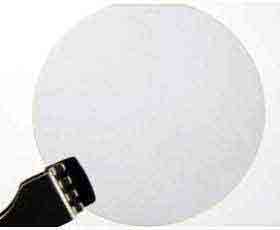
Gallium Nitride Epitaxial Wafers and Substrates
UniversityWafer supplies a selection of gallium nitride (GaN) wafers, GaN epitaxial substrates, and aluminum nitride (AlN) buffer-layer wafers for university laboratories, government research facilities, and commercial semiconductor development.
Available structures include GaN on sapphire, GaN on silicon carbide, GaN/AlN/SiC, and GaN/AlN/Al2O3 epitaxial wafers. These wide-bandgap semiconductor materials are used in LEDs, ultraviolet photodetectors, high-frequency electronics, power devices, sensors, and advanced optoelectronic research.
GaN on 6H-SiC Epitaxial Wafers
GaN on silicon carbide epitaxial wafers consist of an N-type gallium nitride layer grown on a 6H-SiC substrate. Silicon carbide provides high thermal conductivity and is well suited for high-power and high-frequency semiconductor research.
- Wafer diameter: 50 mm
- Substrate: 6H silicon carbide
- Orientation: On-axis
- Conductivity: N-type
- GaN thickness: Approximately 0.5 µm
GaN-on-SiC structures are commonly investigated for RF electronics, high-electron-mobility transistors, power switching devices, microwave components, and high-temperature semiconductor applications.
GaN on Sapphire Epitaxial Wafers
GaN on sapphire wafers combine an epitaxial gallium nitride layer with a sapphire substrate. Sapphire provides electrical insulation, optical transparency, mechanical strength, and compatibility with many GaN growth processes.
- Wafer diameter: 50 mm
- Substrate: Sapphire
- Orientation: On-axis
- Conductivity: N-type GaN
- GaN thickness: Approximately 0.5–10 µm
These wafers are suitable for LED development, ultraviolet photodetectors, optical devices, semiconductor sensors, thin-film characterization, and university research involving wide-bandgap materials.
GaN/AlN/SiC Epitaxial Wafers
A GaN/AlN/SiC epitaxial wafer consists of a gallium nitride layer grown over an aluminum nitride buffer layer on a 6H silicon carbide substrate. The AlN layer can support epitaxial growth and help manage the interface between the GaN film and SiC substrate.
- Wafer diameter: 50 mm
- Substrate: 6H silicon carbide
- Orientation: On-axis
- Conductivity: N-type GaN
- GaN thickness: Approximately 0.5–0.8 µm
- AlN thickness: Approximately 0.1 µm
GaN/AlN/SiC structures may be used for heterostructure research, high-frequency electronics, thermal-management studies, power semiconductor development, and epitaxial material characterization.
GaN/AlN/Al2O3 Epitaxial Wafers
A GaN/AlN/Al2O3 wafer consists of an N-type GaN layer grown over an AlN buffer layer on sapphire. Sapphire is chemically represented as Al2O3.
- Wafer diameter: 50 mm
- Substrate: Sapphire, Al2O3
- Orientation: On-axis
- Conductivity: N-type GaN
- GaN thickness: Approximately 0.5–0.8 µm
- AlN thickness: Approximately 0.1 µm
These epitaxial structures are used in GaN film-growth studies, LEDs, ultraviolet devices, optoelectronics, photodetectors, sensors, and semiconductor process development.
Gallium Nitride Wafer Research Applications
Gallium nitride is a wide-bandgap semiconductor valued for its high breakdown field, high electron mobility, thermal stability, and ability to operate at high voltages, frequencies, and temperatures.
GaN epitaxial wafers are commonly used for:
- Light-emitting diodes and laser diodes
- Ultraviolet photodetectors
- GaN HEMT research
- RF and microwave electronics
- Power semiconductor devices
- High-temperature electronics
- Optoelectronic devices
- Thin-film and interface characterization
- Wide-bandgap semiconductor research
- University semiconductor fabrication projects