
Affordable 200mm Sapphire Wafers for Research
UniversityWafer supplies high-quality 200mm sapphire wafers and 8-inch Al2O3 substrates for semiconductor, LED, RF, photonics, and optoelectronic applications. Our large-diameter C-plane sapphire substrates are available in research quantities as well as larger production lots with custom specifications.
Need a quote? Simply send us your desired thickness, orientation, surface finish, and quantity. Our engineering team can provide fast pricing for standard or custom 200mm epi-ready sapphire wafers.
Get Your 200mm Sapphire Wafer Quote FAST! Or, Buy Online and Start Your Research Today!
25-Wafer Cassette Packaging
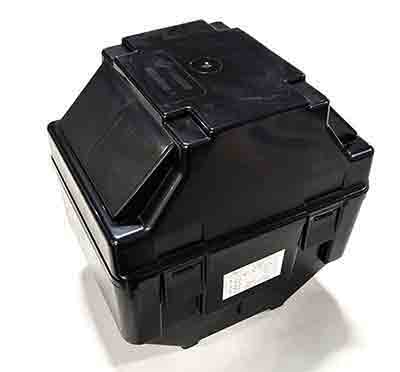
Each 200mm sapphire substrate is packaged in Class 100 cleanroom conditions and vacuum sealed to help protect the polished surfaces during shipping and storage. Standard quantities include 10, 15, 20, and 25 wafers per cassette.
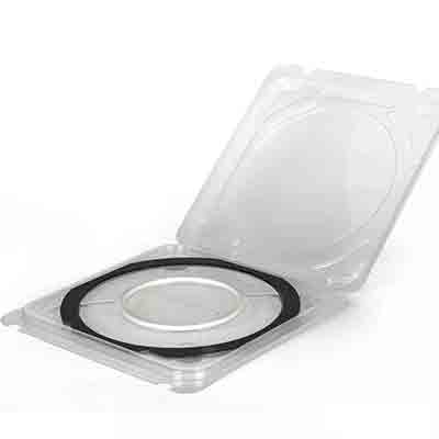
Individual wafer carriers are also available for customers requiring single-wafer handling, inspection, or low-volume research projects.
200mm Sapphire Substrates
UniversityWafer supplies 200mm sapphire wafers, also called 8 inch Al2O3 substrates, for research, pilot production, optoelectronics, LED development, RF devices, and advanced semiconductor applications. These high-purity C-plane sapphire wafers are available in small and larger quantities with epi-polished surfaces and cleanroom cassette packaging.
200mm C-Plane Sapphire Wafer Specifications
- Material: High-purity monocrystalline Al2O3 sapphire, >99.996%
- Diameter: 200.0 ± 0.5mm
- Orientation: C-plane <0001> ± 1°
- Notch Orientation: A-axis <11-20> ± 0.3°
- Notch Depth: 1.0 +0.25/-0.00mm, per SEMI M1-1105
- Notch Angle: 90 +5°/-1°
- Thickness Options: 1.250 ± 0.025mm or 1.515 ± 0.025mm
- Front Surface: Epi-polished, Ra ≤ 0.5nm
- Back Surface: Epi-polished, Ra ≤ 0.5nm
- Edge: Round chamfer / bevel
- TTV: ≤ 20µm
- Bow: ≤ 30µm
- Laser Mark: Back-side scribing or N/A
- Packaging: Class 100 cleanroom, vacuum sealed in single cassette
- Quantities: 10, 15, 20, or 25 wafers
Why Use 200mm Sapphire Wafers?
Sapphire is valued for its excellent hardness, chemical resistance, thermal stability, optical transparency, and electrical insulation. Large-diameter 200mm sapphire substrates help researchers and manufacturers scale processes that require a durable, high-quality wafer platform.
Please send us your required wafer thickness, polish, orientation, quantity, packaging needs, and any custom tolerances. We can quote both small research lots and larger production quantities.
Related Pages
- Sapphire Wafers (Al₂O₃)
- GaN on Sapphire Wafers
- AlGaN on Sapphire Substrates
- HEMT GaN Wafers for High-Frequency Electronics
- Optoelectronic Device Applications
- Integrated Photonics and Optical Circuits
- RF Device Applications
- High-Frequency Electronics Using Sapphire Wafers
- Non-Irradiated Sapphire Wafers