Electronic Wafers for Research and Production
Get Your Quote FAST!
Electronic wafers serve as the foundational building blocks for nearly all modern electronic devices.
Get Your Quote FAST! Or, Buy Online and Start Researching Today!
What Are Electronic Wafers?
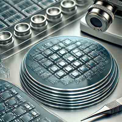
Electronic wafers, also known as semiconductor wafers or simply wafers, are thin, circular slices of semiconductor material (most commonly silicon) used as the substrate for fabricating integrated circuits (ICs), microelectromechanical systems (MEMS), sensors, photonics, and other electronic devices.
Key Features of Electronic Wafers:
- Material: Usually Silicon (Si), but also includes materials like Silicon Carbide (SiC), Gallium
 Arsenide (GaAs), Germanium (Ge), Sapphire (Al₂O₃), or Gallium Nitride (GaN).
 - Shape and Size: Typically round discs with diameters ranging from 1 inch (25 mm) to 12 inches (300 mm), and thicknesses commonly between 200–775 micrometers (µm).
- Surface Finish: They can be single-side polished (SSP), double-side polished (DSP), or etched, depending on the application requirements.
- Crystallographic Orientation: Common orientations include (100), (111), and (110), which influence electronic properties, etching characteristics, and epitaxial growth quality.
Types of Electronic Wafers:
- Undoped (Intrinsic): High purity wafers without intentional doping, used for applications where purity and minimal conductivity are required.
- Doped Wafers: Contain controlled impurities (dopants like boron, phosphorus, arsenic) to create N-type or P-type semiconductors for transistor formation.
- Silicon-on-Insulator (SOI): Wafers that feature a silicon layer separated by a buried oxide (SiO₂) layer, useful in high-performance, low-power electronics.
- Epitaxial Wafers (Epi Wafers): Wafers with a thin crystalline silicon layer grown atop the bulk wafer, providing improved device performance.
Applications:
- Microelectronics: CPUs, memory chips, and microprocessors.
- Sensors and MEMS Devices: Pressure sensors, accelerometers, gyroscopes, optical MEMS.
- Photonics: Laser diodes, LEDs, photovoltaic cells, photodetectors.
- Power Electronics: High-power, high-temperature electronics (using SiC, GaN wafers).
