
How Are Computer Chips Made from Silicon Wafers?
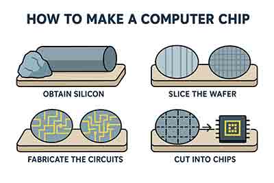
Manufacturing a modern computer chip can require more than 1,000 carefully controlled processing steps. The process begins with high-purity silicon and ends with individual integrated circuits that are tested, packaged, and installed in computers, smartphones, vehicles, medical equipment, and other electronic devices.
A polished silicon wafer serves as the foundation on which thousands of identical chips are fabricated at the same time. Each wafer passes through repeated cycles of cleaning, oxidation, photolithography, doping, deposition, etching, and inspection before it is separated into individual dies.
Ready to Start Making Chips?
Order high-purity silicon wafers today and begin your fabrication process.
Buy Silicon Wafers NowGet Your Quote FAST! Tell us the wafer diameter, thickness, crystal orientation, resistivity, dopant, surface finish, and quantity you need. Or, Buy Online and start researching today.
How Silicon Becomes a Computer Chip
Computer-chip manufacturing begins with electronic-grade silicon. Raw silicon is purified and converted into polysilicon, which is melted and grown into a single-crystal silicon ingot. The ingot is then ground to the required diameter and sliced into thin circular wafers using precision wire-saw equipment.
After slicing, the wafers are lapped, chemically etched, cleaned, and polished to produce an extremely flat surface. Semiconductor-grade wafers may be single-side polished or double-side polished, depending on the process and device requirements. Tight control of total thickness variation, bow, warp, surface roughness, resistivity, and crystal orientation is important for reliable fabrication.
1. Wafer Cleaning and Surface Preparation
Before circuit patterns can be created, the wafer must be thoroughly cleaned. Organic residue, particles, metallic contamination, and native oxide can interfere with later manufacturing steps. Semiconductor facilities therefore use carefully controlled silicon wafer cleaning procedures between many processing stages.
A clean and uniform wafer surface helps photoresist adhere properly, improves film deposition, and reduces defects that could cause individual dies to fail electrical testing.
2. Oxidation and Insulating Layers
A thin layer of silicon dioxide may be grown on the wafer through thermal oxidation. Silicon dioxide acts as an electrical insulator, protective coating, diffusion barrier, and masking material during semiconductor processing.
Engineers can begin with bare silicon or purchase thermal oxide wafers with a specified oxide thickness. Other dielectric materials, including silicon nitride, may be deposited when additional chemical resistance, mechanical strength, or electrical isolation is required.
3. Photolithography Creates the Circuit Pattern
Photolithography transfers microscopic circuit patterns onto the wafer. A light-sensitive chemical called photoresist is applied to the surface, usually by spin coating. The coated wafer is then soft baked to remove excess solvent and stabilize the resist layer.
Ultraviolet light is projected through a patterned photomask or reticle. Depending on whether positive or negative photoresist is used, selected portions of the resist become soluble or remain protected. A developer solution then reveals the required circuit pattern.
The photolithography process is repeated many times because a finished integrated circuit contains multiple transistor, dielectric, contact, and metal-interconnect layers. Advanced devices require extremely accurate alignment between every patterned layer.
4. Etching Removes Selected Material
Once the photoresist pattern has been developed, exposed portions of the underlying film can be removed through wet or dry etching. Wet etching uses liquid chemicals, while plasma-based dry etching provides more directional material removal and is frequently used for very small semiconductor features.
The photoresist protects selected areas while the exposed oxide, nitride, silicon, or metal is removed. After etching, the remaining resist is stripped and the wafer is cleaned before the next layer is processed.
5. Doping Creates P-Type and N-Type Regions
Pure silicon does not yet have the controlled electrical behavior needed to form transistors. Engineers introduce carefully selected dopants to modify its conductivity. Boron is commonly used to create p-type silicon, while phosphorus, arsenic, or antimony may be used to create n-type silicon.
Doping can be performed through thermal diffusion or ion implantation. During ion implantation, charged dopant atoms are accelerated into precisely selected areas of the wafer. A later annealing step repairs crystal damage and electrically activates the dopants.
These patterned p-type and n-type regions form the junctions, channels, wells, sources, and drains required for transistors and other semiconductor devices.
6. Thin-Film Deposition Builds Device Layers
Semiconductor devices are constructed layer by layer. Manufacturers deposit extremely thin films of insulating, semiconducting, and conductive materials using techniques such as chemical vapor deposition, physical vapor deposition, sputtering, evaporation, and atomic layer deposition.
Epitaxial silicon may also be grown on the wafer when the device requires a highly controlled crystalline layer with a specified thickness and dopant concentration.
Specialized substrates such as silicon-on-insulator wafers provide a thin device-quality silicon layer above a buried oxide. SOI technology can improve electrical isolation, reduce parasitic capacitance, and support advanced microelectronics, radio-frequency devices, photonics, and MEMS fabrication.
7. Metal Interconnects Connect the Transistors
Once the transistors have been formed, they must be electrically connected. Conductive materials are deposited and patterned to create microscopic wiring between device components. Multiple interconnect layers may be separated by insulating films and connected through vertical openings called contacts and vias.
Modern integrated circuits can contain many metal layers. These interconnect networks distribute electrical signals, clock signals, ground, and power throughout the chip.
8. Wafer Testing Identifies Working Dies
After wafer fabrication is complete, electrical probe testing is used to evaluate each individual die. Automated probe cards contact small test pads on the wafer and measure whether the circuits operate within their required specifications.
Dies that fail testing are mapped so they can be excluded during assembly. Functional chips may also be sorted into different performance categories according to operating speed, power consumption, voltage, and thermal behavior.
9. Dicing Separates the Individual Chips
The completed wafer contains many repeated rectangular dies separated by narrow streets or scribe lines. Precision wafer dicing separates the wafer into individual chips using a diamond blade, laser, plasma, or another singulation method.
Each working die can then be attached to a package or substrate, electrically connected, sealed for protection, and tested again before shipment.
Why Chip Fabrication Requires a Cleanroom
Semiconductor features are so small that an airborne particle can block a circuit line, damage a transistor, or reduce manufacturing yield. For this reason, chip fabrication takes place in highly controlled cleanrooms with filtered air, regulated temperature, controlled humidity, and strict contamination procedures.
Operators wear protective garments to prevent skin particles, hair, fibers, and other contaminants from reaching the wafer. Process chemicals, equipment, wafer carriers, and tools must also meet strict cleanliness standards.
Why Silicon Crystal Quality Matters
Semiconductor devices are sensitive to crystal defects, contamination, surface damage, and nonuniform electrical properties. The crystalline structure of silicon therefore plays an important role in device performance and fabrication yield.
Researchers and manufacturers select wafers according to parameters such as crystal orientation, dopant type, resistivity, oxygen concentration, carbon concentration, thickness, diameter, flatness, and surface finish. Common orientations include <100>, <110>, and <111>, each of which offers different properties for microelectronics, MEMS, sensors, and other applications.
What Are CPU Wafers?
A CPU wafer is a semiconductor wafer on which many central processing unit dies are fabricated simultaneously. It is not itself a finished CPU. Instead, the wafer contains a repeated grid of processor designs that will later be tested, diced, packaged, and sold as separate chips.
CPU manufacturing commonly uses large-diameter, high-quality silicon wafers because larger wafers can hold more dies and support efficient high-volume fabrication. The exact number of processors per wafer depends on wafer diameter, die dimensions, edge exclusion, process yield, and the number of dies affected by defects.
During fabrication, the CPU wafer undergoes repeated cycles of photolithography, deposition, etching, ion implantation, annealing, chemical-mechanical polishing, cleaning, and metrology. These steps create the transistors, insulating layers, contacts, and metal interconnects required for the processor to perform calculations and move data.
After wafer-level testing, the individual CPU dies are separated and packaged. The finished package protects the die, removes heat, and provides electrical connections between the microscopic circuitry and the computer's circuit board.
Silicon Wafers for Semiconductor Research
UniversityWafer supplies silicon substrates for semiconductor process development, university laboratories, device prototyping, materials research, MEMS, photonics, thin-film deposition, lithography, oxidation, and microelectronics.
Available specifications may include different wafer diameters, thicknesses, crystal orientations, resistivity ranges, dopants, polish types, oxide layers, nitride layers, and custom processing. Researchers can also request research substrates made from silicon carbide, gallium arsenide, gallium nitride, sapphire, germanium, glass, quartz, and other advanced materials.
What Is a Semiconductor?
A semiconductor is a material whose electrical conductivity falls between that of a conductor and an insulator. By carefully controlling its electrical properties through doping, engineers can create transistors, integrated circuits, sensors, power devices, and photonic components. The most widely used semiconductor is silicon, although materials such as silicon carbide (SiC), gallium arsenide (GaAs), and gallium nitride (GaN) are widely used for specialized applications.
Modern semiconductor manufacturing begins with ultra-high-purity polysilicon. The silicon is melted and grown into a large single-crystal ingot using the Czochralski process. This produces the highly ordered crystal structure required for advanced semiconductor fabrication.
From Silicon Ingot to Silicon Wafer
Once the crystal has been grown, the silicon ingot is inspected, ground to the required diameter, and sliced into thin silicon wafers using precision wire saws. Material removed during cutting is known as kerf loss, which manufacturers continually work to reduce through improved sawing technologies and kerfless wafer production methods.
After slicing, every wafer is lapped, etched, polished, and cleaned to create the extremely flat, defect-free surface required for integrated circuits (ICs), MEMS devices, sensors, and photonic components.
Photolithography and Chip Fabrication
The fabrication of computer chips requires dozens of repeated processing cycles. During photolithography, light-sensitive photoresist is applied to the wafer and exposed through a mask that transfers microscopic circuit patterns onto the surface.
Each fabrication cycle may include oxidation, deposition, ion implantation, etching, cleaning, and epitaxial growth. Advanced processors often require dozens of lithography steps before the finished chips are tested, diced, packaged, and assembled into electronic products.
Additional Semiconductor Manufacturing Processes
Although photolithography is one of the most recognizable steps in semiconductor manufacturing, dozens of additional fabrication processes are required before a silicon wafer becomes a functioning computer chip. Each processing cycle builds new microscopic structures that eventually form billions of interconnected transistors.
One of the first steps after patterning is thermal oxidation, where a thin layer of silicon dioxide is grown on the wafer surface. This insulating layer is essential for MOSFET devices and integrated circuits. Depending on the application, manufacturers may use thermal oxide wafers or deposit other dielectric materials such as silicon nitride.
Engineers then modify the electrical properties of the wafer using ion implantation or diffusion. Carefully selected dopants such as boron, phosphorus, or arsenic create p-type and n-type regions that allow individual transistors to switch electrical current on and off with remarkable precision.
As manufacturing progresses, multiple layers of conductive metals and insulating films are deposited onto the wafer. Thin-film deposition techniques, including chemical vapor deposition (CVD), physical vapor deposition (PVD), sputtering, and atomic layer deposition (ALD), are commonly used to build these ultra-thin layers with nanometer-scale precision.
After every deposition step, advanced etching processes remove unwanted material while preserving the intricate circuit patterns created during photolithography. These fabrication cycles are repeated dozens of times until the finished integrated circuit contains multiple metal layers connected through microscopic vias.
Once fabrication is complete, each wafer undergoes extensive electrical testing before it is cut into individual dies using precision wafer dicing equipment. The working chips are then packaged, tested again, and incorporated into products ranging from smartphones and laptops to medical devices, automotive electronics, artificial intelligence accelerators, and aerospace systems.
Modern semiconductor fabrication facilities can manufacture thousands of chips simultaneously on a single silicon wafer, making wafer-level processing one of the most efficient manufacturing methods ever developed. Researchers also fabricate devices on specialized substrates such as SOI wafers, silicon carbide, gallium arsenide, and gallium nitride for applications that require higher power, faster switching speeds, or improved optical performance.
Why Cleanrooms Are Essential
Semiconductor manufacturing takes place inside ultra-clean fabrication facilities where airborne contamination is tightly controlled. Even microscopic dust particles can damage a transistor or interrupt a circuit. This is why wafers undergo repeated cleaning processes between manufacturing steps to maintain extremely high yields.
What Does a Silicon Wafer Look Like?
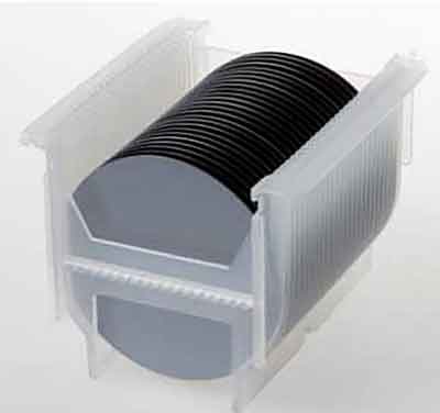 A silicon wafer is a thin circular disc with an extremely smooth mirror-like surface. Wafers are available in many diameters, including 2", 3", 4", 100 mm, 150 mm, 200 mm, and 300 mm, as well as custom thicknesses, crystal orientations, dopants, and surface finishes for research and production applications.
Researchers also use specialized substrates such as SOI wafers, thermal oxide wafers, silicon nitride wafers, sapphire wafers, and germanium wafers depending on device requirements.
How Many Chips Fit on a Wafer?
The number of chips produced from a wafer depends primarily on the wafer diameter and the size of each individual die. Larger wafers, such as 300 mm silicon wafers, allow manufacturers to fabricate significantly more chips than smaller wafers, improving manufacturing efficiency while reducing cost per device.
What Is a Microchip?
A microchip, also called an integrated circuit (IC), is fabricated by building multiple microscopic layers on a semiconductor wafer. Modern processors contain billions of transistors connected through extremely small metal interconnects created during repeated photolithography and deposition processes.

Today's microchips power computers, smartphones, automobiles, medical devices, artificial intelligence hardware, telecommunications equipment, industrial automation, and countless consumer electronics. As manufacturing technology advances, transistors continue to shrink while computing performance and energy efficiency continue to improve.