Integrated Silicon III-V Chips for Advanced Semiconductor Devices
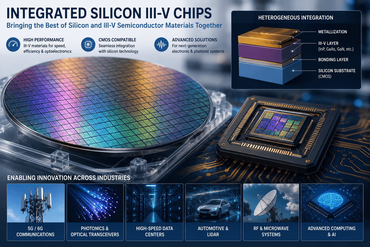
Integrated Silicon III-V chips combine the scalability of silicon CMOS with the exceptional optical and electronic performance of III-V semiconductor materials such as GaAs, GaN, and InP and other III-V compounds. These heterogeneous integration technologies enable high-speed optical communications, silicon photonics, AI hardware, RF electronics, quantum devices, and next-generation semiconductor systems by leveraging the strengths of both silicon and compound semiconductors.
Get Your Silicon & III-V Wafer Quote FAST!
UniversityWafer supplies the silicon wafers, III-V semiconductor substrates,
and epitaxial materials used to develop the next generation of
integrated silicon III-V chips. Researchers worldwide rely on our substrates
to fabricate photonic integrated circuits (PICs), on-chip lasers, high-speed
electronics, RF devices, quantum technologies, and advanced optoelectronic
systems.
Whether you are integrating GaAs, InP,
GaN, or other III-V materials with silicon CMOS technology,
our engineering team can help you select the appropriate substrate,
orientation, resistivity, thickness, surface finish, and epitaxial structure
for your research or production requirements.
Recent Research Inquiry
"Our laboratory is developing heterogeneous silicon photonic chips with
integrated InP laser sources. We are looking for 100 mm silicon wafers and
III-V epitaxial structures suitable for wafer bonding. Can you provide
available substrate specifications, bonding surface quality, and prototype
pricing?"
Available Materials
- Silicon (Si) wafers
- Silicon-on-Insulator (SOI) wafers
- Gallium Arsenide (GaAs)
- Gallium Nitride (GaN)
- Indium Phosphide (InP)
- Indium Arsenide (InAs)
- Gallium Antimonide (GaSb)
- Custom III-V epitaxial wafers
- Double-side polished wafers
- Prime and test grade substrates
Applications
Integrated silicon III-V technologies are widely used in silicon photonics,
high-speed optical communications, quantum computing, RF and microwave
electronics, LiDAR, optical sensing, AI hardware, data centers, advanced
microelectronics, and next-generation semiconductor devices.
Complete the quotation form with your desired substrate material, wafer
diameter, crystal orientation, doping type, resistivity, thickness, epitaxial
requirements, and quantity. Our engineers will recommend the best solution and
provide a fast quotation for your research project.
Get Your Quote FAST! Or,
Buy Online
and Start Your Research Today!
What Are Integrated Silicon III-V Chips?
Integrated silicon III-V chips combine the manufacturing
advantages of silicon with the superior optical and electronic properties of
III-V compound semiconductors such as gallium arsenide (GaAs),
indium phosphide (InP), gallium nitride (GaN), indium arsenide (InAs), and
gallium antimonide (GaSb). This heterogeneous integration enables a single
chip to perform functions that conventional silicon alone cannot achieve,
including efficient light generation, high-speed optical communication, and
high-frequency signal processing.
As artificial intelligence, cloud computing, quantum technologies, and
high-speed networking continue to evolve, silicon III-V integration has become
one of the fastest-growing areas of semiconductor research. UniversityWafer
supplies the silicon, SOI, III-V substrates, and epitaxial wafers used to
develop these next-generation devices.
Why Combine Silicon and III-V Semiconductors?
| Technology |
Key Advantages |
Typical Applications |
| Silicon (Si) |
Low-cost manufacturing, mature CMOS processing, high integration density, and excellent mechanical stability. |
Processors, memory, sensors, CMOS integrated circuits, MEMS, and silicon photonics. |
| III-V Semiconductors |
Direct bandgap materials with superior optical emission, high electron mobility, and excellent high-frequency performance. |
Lasers, LEDs, photodetectors, RF electronics, high-speed communications, and quantum devices. |
| Integrated Silicon III-V Chips |
Combines silicon scalability with III-V optical and electronic performance on a single platform. |
Photonic integrated circuits (PICs), optical interconnects, AI hardware, LiDAR, and advanced communication systems. |
Common III-V Materials Used
Several III-V semiconductor materials are integrated with silicon depending on
the desired device performance:
- Gallium Arsenide (GaAs) — High-speed electronics, RF devices, and photodetectors.
- Indium Phosphide (InP) — Optical communication lasers, modulators, and photonic integrated circuits.
- Gallium Nitride (GaN) — Power electronics, RF amplifiers, LEDs, and high-power devices.
- Indium Arsenide (InAs) — Infrared detectors and high-mobility electronic devices.
- Gallium Antimonide (GaSb) — Mid-infrared lasers, sensors, and infrared optoelectronics.
Integration Technologies
Researchers use several techniques to integrate silicon and III-V materials,
each offering unique advantages depending on the application and manufacturing
requirements.
- Direct wafer bonding
- Die-to-wafer bonding
- Heterogeneous integration
- Monolithic epitaxial growth
- Flip-chip bonding
- Micro-transfer printing
- Hybrid photonic integration
Applications of Integrated Silicon III-V Chips
Silicon III-V integration enables high-performance devices that combine
advanced electronics with optical functionality on a compact semiconductor
platform.
- Silicon photonics
- Photonic integrated circuits (PICs)
- Optical transceivers
- On-chip lasers
- High-speed optical communications
- Artificial intelligence accelerators
- Quantum computing hardware
- LiDAR systems
- RF and microwave electronics
- Data center interconnects
- Advanced sensing technologies
- Power electronics
Silicon and III-V Substrates for Research
UniversityWafer supplies research-grade and production-quality silicon, SOI,
GaAs, InP, GaN, InAs, GaSb, and custom epitaxial wafers for heterogeneous
integration projects. Available options include custom diameters, crystal
orientations, resistivity ranges, doping types, epitaxial structures,
double-side polishing, and application-specific substrate specifications to
support photonics, microelectronics, quantum research, and next-generation
semiconductor development.
Related Pages
