
I am looking for germanium on silicon wafers. Ideally, I would like a 100 mm (4-inch) wafer with a 5–10 µm germanium layer. Depending on the price, I would like to order between four and ten wafers.
Substrates for Lab-on-a-Chip and Microfluidic Device Research
Lab-on-a-Chip (LOC) devices combine microfluidics, MEMS, biosensors, and semiconductor fabrication technologies on a single platform to perform chemical, biological, and diagnostic analyses. The choice of substrate is critical because it determines optical performance, chemical resistance, thermal properties, and compatibility with CMOS processing. Common materials include silicon wafers, glass, polymers, and germanium-based substrates.
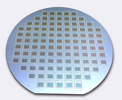
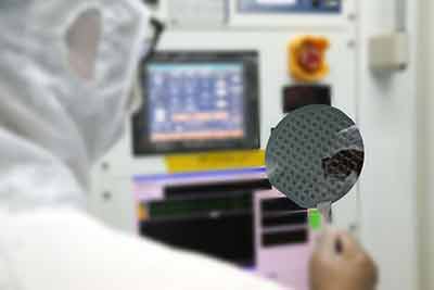
Germanium-on-Silicon Wafers for Lab-on-a-Chip Research
A PhD student working with a Lab-on-a-Chip research group requested the following:
UniversityWafer Solution
Germanium can be deposited on silicon using physical vapor deposition (PVD). Amorphous germanium coatings are available without requiring additional interlayers between Ge and Si.
- Substrate material: Silicon
- Optical coating: Customizable
- Solder alloy: Au80Sn20 or custom alloy
- Wafer sizes: 6-inch and 8-inch
- Surface quality: 40/20 or 20/10
- Humidity and temperature testing: >500 hours at 85% RH and 85°C
Reference #245401 for specifications and pricing.
Why Silicon Wafers Are Used for Lab-on-a-Chip Devices
The foundation of many lab-on-a-chip systems is CMOS technology, which allows integration of microelectronics, MEMS devices, and microfluidic channels onto a single platform. Silicon offers several advantages:
- Excellent mechanical strength
- High thermal stability
- Compatibility with MEMS fabrication
- CMOS process integration
- High aspect-ratio structures through DRIE etching
- Large-scale manufacturing capability
Common Substrates Used in Lab-on-a-Chip Fabrication
- Silicon wafers
- Glass wafers
- Quartz substrates
- PDMS polymer substrates
- PMMA substrates
- Germanium-on-Silicon (Ge-on-Si)
- Germanium-on-Insulator (GeOI) wafers
Applications of Lab-on-a-Chip Platforms
- Point-of-care diagnostics
- Microfluidics and biosensors
- DNA sequencing
- Cell analysis and sorting
- Drug discovery
- Virus detection
- Photonic sensors
- Biomedical engineering
- Environmental monitoring
Double-Side Polished Silicon Wafers for LOC Devices
Researchers have also used double-side polished (DSP) silicon wafers for Lab-on-a-Chip fabrication because they provide excellent surface flatness and facilitate bonding to glass or polymer layers.
Reference #2494226. Contact us for complete specifications and inventory availability.
Get Your Quote FAST! Or Buy Online and start researching today.
What Is Lab-on-a-Chip Technology?
 Lab-on-a-Chip (LOC) technology integrates multiple laboratory functions onto a microchip only a few square centimeters in size. These devices combine microfluidics, MEMS, sensors, and semiconductor fabrication techniques to perform chemical and biological analysis using extremely small sample volumes.
Lab-on-a-chip systems are widely used in point-of-care diagnostics, DNA analysis, drug discovery, biosensors, and environmental monitoring.
Applications of Lab-on-a-Chip Devices
- Point-of-care diagnostics
- DNA and RNA analysis
- Virus detection and biosensors
- Drug discovery and pharmaceutical research
- Cancer diagnostics
- Cell sorting and cell culture
- Environmental monitoring
- Food safety testing
- Microfluidic devices
- Wearable biosensors
Advantages of Lab-on-a-Chip Platforms
- Reduced sample volume requirements
- Fast analysis and response times
- Lower reagent consumption
- Portable diagnostic systems
- High throughput screening
- Lower manufacturing costs
- Improved sensitivity and accuracy
- Integration with CMOS and MEMS technologies

Substrates Commonly Used for Lab-on-a-Chip Devices
Several substrate materials are used to fabricate lab-on-a-chip platforms depending on the application.
| Material | Advantages |
|---|---|
| Silicon | MEMS compatibility, excellent mechanical properties |
| Glass | Optical transparency and chemical resistance |
| PDMS | Low cost and easy fabrication |
| PMMA | Disposable and biocompatible |
| Germanium-on-Silicon | Integrated photonic and optoelectronic devices |
Microfluidics and Biosensors
Modern lab-on-a-chip devices frequently incorporate biosensors, optical detectors, and microfluidic channels. These systems can analyze biological samples with high sensitivity while minimizing reagent consumption and processing time.
Silicon Wafers for Lab-on-a-Chip Fabrication
Silicon remains one of the most widely used materials for lab-on-a-chip fabrication because it is compatible with CMOS technology, MEMS devices, and advanced etching processes such as DRIE. Silicon wafers can be bonded to glass or polymer layers to create highly integrated microfluidic systems.

Future of Lab-on-a-Chip Technology
Lab-on-a-chip devices are expected to transform healthcare, personalized medicine, and biomedical research. Advances in microfluidics, nanotechnology, photonics, and semiconductor manufacturing continue to drive the development of faster, smaller, and more sensitive diagnostic systems.