
Silicon Wafers for PhD Microchannel Etching Research
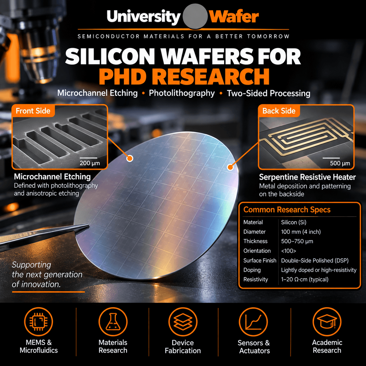
A PhD researcher requested double-side polished (DSP) silicon wafers for a microfabrication project involving microchannel etching on one side of the wafer and a serpentine resistive heater on the opposite side.
The researcher plans to use photolithography to define the microchannel structures before etching the silicon substrate.

Requested Silicon Wafer Specifications
- Material: Silicon (Si)
- Diameter: 100 mm (4 inch)
- Thickness: 500–750 µm
- Crystal Orientation: <100>
- Surface Finish: Double-Side Polished (DSP)
- Doping: Lightly doped or high-resistivity silicon requested
- Resistivity: 1–20 Ω·cm requested
Reference #318810 for specifications and pricing.
Why Use Double-Side Polished Silicon?
DSP silicon provides polished surfaces on both sides of the wafer, making it useful for research projects that require fabrication or characterization on both the front and backside of the substrate.
In this application, one side can be processed for microchannels, while the opposite side can support patterned metal structures such as a resistive heater. Wafer thickness, orientation, resistivity, and surface finish should be selected according to the specific etching, deposition, and electrical requirements of the device.
Need Silicon Wafers for Your PhD Research?
UniversityWafer supplies silicon wafers for university laboratories, graduate research, prototype fabrication, MEMS, microfluidics, photolithography, thin-film deposition, and other experimental applications.
Send us your required diameter, thickness, crystal orientation, doping type, resistivity, surface finish, coatings, and quantity. If you do not know the exact wafer specification, include information about your intended fabrication process or application.
Get Your Research Wafer Quote FAST! Or, Buy Online and Start Researching Today!
Silicon Wafers for PhD Research and Microfabrication
PhD researchers in materials science, electrical engineering, physics, chemistry, MEMS, and related fields often use semiconductor wafers as controlled substrates for fabrication and characterization experiments. Silicon is especially common because researchers can specify properties such as crystal orientation, thickness, doping, resistivity, surface finish, and oxide layers to match the requirements of an experiment.
Choosing a Silicon Wafer for Research
There is no single silicon wafer specification that is ideal for every research project. The correct substrate depends on the fabrication process, device design, measurement method, and required electrical or mechanical properties.
Important wafer specifications may include:
- Diameter: Common research sizes include 25.4 mm, 50.8 mm, 76.2 mm, 100 mm, 150 mm, 200 mm, and larger wafers.
- Crystal orientation: Orientations such as <100> and <111> influence the crystallographic surface and can be especially important when anisotropic silicon etching is involved.
- Thickness: Wafer thickness affects mechanical handling, device geometry, through-wafer processing, and compatibility with fabrication equipment.
- Doping and resistivity: P-type, N-type, lightly doped, highly doped, and high-resistivity silicon are available for different electrical and device requirements.
- Surface finish: Single-side polished (SSP) wafers are suitable for many processes, while double-side polished (DSP) wafers provide polished surfaces on both sides for research requiring backside processing, optical access, or processing on both wafer surfaces.
Why Use <100> Silicon for Microchannel Etching?
<100> silicon is widely used in silicon bulk micromachining. When silicon is etched with an anisotropic wet etchant such as potassium hydroxide (KOH), different crystallographic planes etch at different rates. In a (100) silicon wafer, the slowly etched {111} planes can define the angled sidewalls of etched cavities and channels.
Because the final geometry depends on crystal orientation, researchers designing microchannels, cavities, membranes, and related MEMS structures should select the wafer orientation together with the etching process and desired device geometry.
Double-Side Polished Silicon for Two-Sided Processing
Double-side polished (DSP) silicon wafers have polished surfaces on both sides. This makes them useful when a research process involves features or fabrication steps on both the front and back of the substrate.
For example, a researcher may fabricate microchannels on one side of a silicon wafer while forming metal structures, sensors, heaters, or other device features on the opposite side. DSP substrates are also useful when backside alignment or optical inspection through the processing setup is required.
Photolithography and Silicon Micromachining
Photolithography is commonly used to transfer patterns from a photomask into a photoresist layer on the wafer. The patterned resist can then help define regions for subsequent etching, deposition, implantation, or other microfabrication steps.
For deep anisotropic wet etching of silicon, researchers must also consider the compatibility and durability of the selected etch-mask material. Silicon nitride is commonly used as a masking material for anisotropic silicon wet etching because of its relatively low etch rate in many anisotropic etchants.
Silicon Wafers for Resistive Heaters and Sensors
Silicon substrates can support patterned metal structures used as resistive heaters, temperature sensors, electrodes, and other microfabricated components. Metal films can be deposited and patterned using fabrication methods selected according to the required materials, dimensions, adhesion, temperature range, and electrical performance.
When microchannels and electrical structures are fabricated on opposite sides of the same wafer, substrate thickness, surface finish, alignment, electrical isolation, and the order of fabrication steps all become important process-design considerations.
Other Substrates Used in PhD Research
Although silicon is one of the most widely used research substrates, UniversityWafer supplies materials for many different experimental requirements. Depending on the application, researchers may use silicon-on-insulator (SOI), fused silica, quartz, sapphire, silicon carbide (SiC), gallium arsenide (GaAs), gallium nitride (GaN), germanium, or glass substrates.
Material selection should be based on the electrical, optical, thermal, mechanical, and chemical requirements of the experiment rather than on a single general-purpose wafer specification.
Ordering Wafers for University Research
When requesting wafers for a PhD project, provide as much information as possible about the substrate and fabrication process. Useful specifications include material, diameter, thickness, crystal orientation, doping type, resistivity, surface finish, oxide or film requirements, and quantity.
If the exact wafer specification is not known, describing the intended fabrication process—such as photolithography, wet etching, thin-film deposition, MEMS fabrication, or electrical testing—can help identify suitable substrate options.