
SOI Wafers for Silicon Photonics Research
Silicon-on-Insulator (SOI) wafers are the preferred substrate for many modern photonic devices, including optical waveguides, photonic integrated circuits (PICs), modulators, optical switches, ring resonators, and photodiodes. The combination of a thin silicon device layer and a buried oxide layer provides excellent optical confinement, making SOI one of the most important platforms for silicon photonics development.
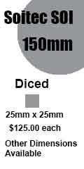
To support university, government, and industrial research programs, UniversityWafer offers diced SOITEC SOI wafers that provide access to premium photonics-grade substrates without the cost of purchasing an entire wafer.
SOITEC SOI Wafer Specifications for Photonic Device Fabrication
The following SOI substrate is commonly used for silicon photonics and optical device research:
- Material: Silicon-On-Insulator (SOI)
- Size: 25 mm × 25 mm diced die
- Orientation: P-type (100)
- Resistivity: 10–20 Ω-cm
- Handle Wafer Thickness: 500 µm
- Device Layer Thickness: 220 nm
- Buried Oxide (BOX): 3 µm
- Polish: Single-Side Polished (SSP)
The 220 nm silicon device layer is one of the most widely used thicknesses in silicon photonics because it supports efficient optical waveguide fabrication and operation at telecommunications wavelengths near 1310 nm and 1550 nm.
Applications of SOI Wafers in Photonics
Researchers use SOI wafers to fabricate:
- Silicon optical waveguides
- Photonic integrated circuits (PICs)
- Optical modulators
- Photodiodes
- Ring resonators
- Optical filters
- Optical switches
- Fiber-optic communication devices
- Quantum photonic devices
- Integrated optical sensors
Because SOI wafers are compatible with CMOS semiconductor manufacturing processes, they enable scalable fabrication of advanced photonic systems while reducing development costs and accelerating commercialization.
Get Your SOI Wafer Quote FAST! Or, Buy SOI Wafers Online and Start Researching Today!
How Are SOI Wafers Used to Fabricate Photonic Devices?
Silicon-on-insulator (SOI) wafers are the foundation of modern silicon photonics. Their unique structure consists of a thin silicon device layer positioned above a buried oxide (BOX) layer and a silicon handle wafer. This architecture provides excellent optical confinement, low propagation loss, and compatibility with standard CMOS fabrication processes.
SOI wafers are widely used to fabricate photonic integrated circuits (PICs), optical waveguides, modulators, photodiodes, optical switches, ring resonators, multiplexers, and other high-performance photonic components. The buried oxide layer prevents optical energy from leaking into the substrate, enabling efficient light transmission and compact device designs.
Why SOI Is the Preferred Platform for Silicon Photonics
The high refractive index contrast between silicon and silicon dioxide allows engineers to create extremely compact optical structures with tight light confinement. This enables the fabrication of miniature photonic devices that can be integrated directly with electronic circuits.
Key advantages of SOI wafers include:
- Low optical propagation loss
- Excellent optical confinement
- CMOS-compatible processing
- High integration density
- Reduced device footprint
- Low power consumption
- Scalable wafer-level manufacturing
- Compatibility with telecommunications wavelengths
Fabrication of Silicon Photonic Waveguides
One of the most common silicon photonics structures is the rib waveguide or strip waveguide. Fabrication typically begins with a thin silicon device layer, often 220 nm thick, deposited on top of a buried oxide layer. Using advanced lithography and dry etching techniques, the silicon layer is patterned to create optical waveguides capable of guiding light with minimal loss.
The resulting waveguides form the building blocks of more complex photonic systems, including:
- Optical modulators
- Photonic switches
- Optical filters
- Ring resonators
- Beam splitters
- Photonic sensors
- Photonic integrated circuits (PICs)
SOI Photodiodes and Optical Detectors
SOI substrates are also used to manufacture high-performance photodiodes and optical detectors. These devices convert incoming light into electrical signals and play a critical role in optical communications, LiDAR systems, imaging technologies, and sensing applications.
The excellent material quality and isolation provided by the buried oxide layer help reduce parasitic effects, improve responsivity, and lower dark current compared with conventional bulk silicon devices.
Applications of Silicon Photonics
SOI-based photonic devices are used throughout modern technology, including:
- Fiber-optic telecommunications
- Data center optical interconnects
- Artificial intelligence hardware
- High-speed optical communications
- LiDAR systems
- Biomedical sensors
- Quantum photonics research
- Integrated optical computing
- Environmental monitoring
- Defense and aerospace systems
Common SOI Wafer Specifications for Photonics
Many silicon photonics researchers utilize SOI wafers with a 220 nm silicon device layer and a 2–3 µm buried oxide layer. These dimensions provide excellent optical confinement for devices operating at telecommunications wavelengths near 1310 nm and 1550 nm.
Whether developing photonic integrated circuits, optical transceivers, modulators, or advanced sensing technologies, SOI wafers remain one of the most important substrate platforms for next-generation photonic device fabrication.
Related Silicon Photonics Resources
- SOI Wafers
- Silicon Wafers
- Photonic Devices
- Optoelectronic Devices
- Indium Phosphide (InP) Wafers
- Gallium Arsenide (GaAs) Wafers
- Gallium Nitride (GaN) Wafers
- Thermal Oxide Silicon Wafers
- Electron Beam Evaporation
- Dry Etching
- Scanning Tunneling Microscopy
- Microfluidic Substrates
- Sapphire Wafers
- Thin Film Deposition