How Is Thermal Oxide Leakage Measured?
Thermal oxide silicon wafers are widely used in semiconductor manufacturing, MEMS fabrication, photolithography, wafer bonding, and microelectronic device development. Researchers frequently compare thermal oxide wafers, dry thermal oxide, and wet thermal oxide processes to optimize leakage current, dielectric strength, breakdown voltage, and gate oxide reliability. High-quality silicon dioxide (SiO₂) layers provide excellent electrical insulation for MOSFETs, CMOS circuits, sensors, and advanced semiconductor devices where low leakage and long-term stability are critical.
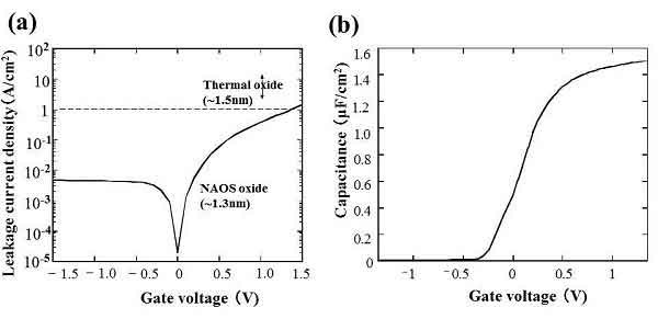
Thermal Oxide Leakage in Silicon Wafers
Thermal oxide wafers are widely used in semiconductor manufacturing, MEMS fabrication, photolithography, wafer bonding, and integrated circuit production. One of the most important characteristics of a thermal oxide layer is its ability to provide electrical insulation while minimizing leakage current. Researchers frequently compare wet thermal oxide and dry thermal oxide when selecting substrates for gate oxides, isolation layers, and dielectric applications.
Scientist Question:
Q. How is the leakage performance of thermal oxide wafers?
A. Wet thermal oxide is generally not intended for high-performance insulation or gate dielectric applications. It is commonly used as a photolithography masking layer and for thick oxide growth where electrical isolation is not the primary concern. Because wet oxide can be less dense than dry oxide, it may exhibit higher leakage current under certain operating conditions.
For applications requiring superior insulation, low leakage current, and high dielectric reliability, researchers often select dry thermal oxide, particularly dry thermal chlorinated oxide. A 300 nm dry thermal oxide layer is typically sufficient for many isolation and gate oxide applications. Premium dry chlorinated oxides combined with a forming gas anneal can further improve interface quality and reduce defect-related leakage.
Reference: Thermal Oxide Leakage Inquiry
Get Your Thermal Oxide Wafer Quote FAST! Or, Buy Online and Start Researching Today!
Wet Thermal Oxide vs. Dry Thermal Oxide
The choice between wet and dry oxidation depends on the intended application. Wet thermal oxide grows more rapidly and is often used when thicker oxide layers are required. Dry thermal oxide grows more slowly but generally produces denser silicon dioxide films with improved electrical properties, lower defect density, and enhanced dielectric performance.
- Wet Thermal Oxide: Faster growth rate, commonly used for field oxides and photolithography masking.
- Dry Thermal Oxide: Lower leakage current, higher dielectric strength, and improved gate oxide integrity.
- Dry Chlorinated Oxide: Enhanced oxide quality and reduced contamination for advanced semiconductor devices.
- Forming Gas Annealed Oxide: Reduced interface defects and improved electrical reliability.
Applications of Thermal Oxide Silicon Wafers
Thermal oxide silicon wafers are commonly used in:
- CMOS and MOSFET fabrication
- MEMS device manufacturing
- Photolithography masking
- Microfluidic device fabrication
- Wafer bonding processes
- Electrical isolation layers
- Sensor development
- Semiconductor research and prototyping
Leakage current and breakdown voltage can vary significantly depending on wafer processing conditions, oxide thickness, thermal treatment, contamination levels, and testing methodology. As a result, exact leakage specifications are often application-dependent and must be evaluated within the customer's process flow.
What Is Thermal Oxide Leakage?
Thermal oxide leakage refers to the unwanted flow of electrical current through a silicon dioxide (SiO₂) layer grown on a silicon wafer. Leakage current becomes increasingly important in semiconductor devices as oxide thickness decreases and electric field strength increases. Thermal oxide layers are commonly used as gate dielectrics, isolation layers, masking layers, and surface passivation coatings in microelectronics and MEMS fabrication.
The amount of leakage depends on several factors, including oxide thickness, growth method, surface cleanliness, crystal quality, operating voltage, and post-oxidation processing. Engineers often evaluate leakage current when selecting wafers for MOSFET fabrication, integrated circuits, sensors, and high-voltage semiconductor devices.
Wet Thermal Oxide vs. Dry Thermal Oxide
The two most common thermal oxidation processes are wet oxidation and dry oxidation.
Wet thermal oxide is produced using water vapor during oxidation. It grows faster than dry oxide and is commonly used when thicker oxide layers are required. Wet oxide is often selected for field oxides, isolation layers, and photolithography masking applications.
Dry thermal oxide is grown using pure oxygen. Although growth rates are slower, dry oxide generally produces denser films with improved electrical characteristics, lower defect concentrations, higher dielectric strength, and reduced leakage current.
For critical gate oxide applications, many researchers prefer dry thermal oxide wafers or dry chlorinated oxide because they provide superior insulation and improved long-term reliability.
How Is Thermal Oxide Leakage Measured?
Leakage current is typically measured by applying a voltage across the oxide layer and monitoring the resulting current flow. Common parameters used to evaluate thermal oxide quality include:
- Leakage current density (A/cm²)
- Breakdown voltage
- Dielectric strength
- Oxide charge density
- Interface trap density
- Gate oxide integrity (GOI)
- Time-dependent dielectric breakdown (TDDB)
These measurements help determine whether an oxide layer is suitable for advanced semiconductor fabrication, high-voltage electronics, and integrated circuit manufacturing.
Gate Oxide Leakage in MOS Devices
As MOSFET gate oxides become thinner, electron tunneling through the dielectric increases. This phenomenon is known as gate oxide leakage. Excessive leakage current can increase power consumption, reduce device reliability, generate heat, and limit transistor scaling.
To minimize leakage, semiconductor manufacturers often optimize oxide growth conditions, perform forming gas anneals, introduce nitrogen into the dielectric, or utilize advanced high-k dielectric materials.
Benefits of Thermal Oxide on Silicon Wafers
- Excellent silicon surface passivation
- High dielectric strength
- Uniform oxide thickness
- Strong adhesion to silicon
- Compatibility with semiconductor manufacturing
- Excellent photolithography masking properties
- Improved device reliability
- Low interface defect density
Applications of Thermal Oxide Wafers
Thermal oxide wafers are widely used in:
- MOSFET fabrication
- CMOS integrated circuits
- MEMS devices
- Microfluidics
- Photolithography masking
- Wafer bonding
- Optical sensors
- Power electronics
- Research and development
For applications requiring the lowest leakage current and highest dielectric reliability, researchers frequently select dry thermal oxide or chlorinated thermal oxide wafers grown under carefully controlled oxidation conditions.
Related Thermal Oxide Resources
