
Order Low-TTV and Ultra-Flat Silicon Wafers
UniversityWafer supplies low-TTV and ultra-flat silicon wafers for photolithography, wafer bonding, advanced packaging, photonics, and MEMS fabrication .
Available options may include double-side-polished (DSP) wafers , prime-grade silicon , and ultra-flat wafers selected for applications requiring controlled thickness and wafer geometry.
Selecting the Correct Specification
TTV requirements should be selected according to the process and measurement method rather than by wafer grade alone. When requesting a quote, identify the geometric properties that are critical to your application.
- Wafer diameter and nominal thickness
- Maximum allowable TTV or GBIR
- Bow and warp limits, when applicable
- Site-flatness requirement and measurement-site size
- Edge-exclusion requirement
- Single-side-polished or double-side-polished finish
- Surface-roughness requirement
- Crystal orientation, dopant type, and resistivity
- Required quantity and documentation
Specifications such as TTV below 1 µm or 2 µm may be available for certain wafer diameters and configurations. Availability depends on wafer size, thickness, polishing, measurement conditions, quantity, and manufacturing capability.
Common Applications
- Photolithography: Controlled geometry can support consistent chucking, alignment, and focus.
- Wafer bonding: Low TTV, controlled bow and warp, and suitable surface quality help promote uniform contact between wafers.
- MEMS: Thickness uniformity can improve dimensional control during etching, membrane formation, and cavity fabrication.
- Optical and photonic devices: Flat, polished substrates can support accurate alignment and controlled optical interfaces.
- Advanced packaging: Controlled wafer geometry can assist with thinning, bonding, stacking, and layer-transfer processes.
Get Your Ultra-Flat Silicon Wafer Quote FAST! Or, Buy Online and start researching today.
Understanding Silicon Wafer TTV and Flatness
Total thickness variation and wafer flatness affect how consistently a silicon wafer can be processed, aligned, bonded, and measured. Although these specifications are related, they describe different geometric characteristics and should not be treated as interchangeable.
| Question | Short Answer |
|---|---|
| Is TTV the same as bow or warp? | No. TTV describes thickness variation. Bow and warp describe free-state wafer shape or curvature. |
| Does low TTV guarantee good lithography? | Not by itself. Lithography may also depend on site flatness, bow, warp, chucking conditions, surface quality, and equipment depth of focus. |
| When are ultra-flat wafers useful? | They are commonly considered for precision lithography, wafer bonding, MEMS, optical devices, metrology, and other processes that require consistent wafer geometry. |
What Is Total Thickness Variation?
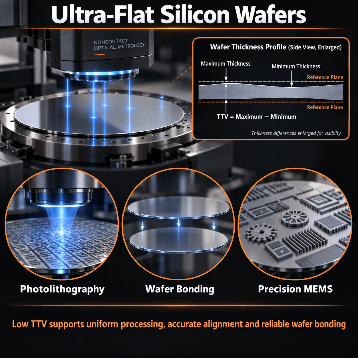
Total thickness variation (TTV) is the difference between the maximum and minimum thickness measured across a wafer within a defined measurement area:
TTV = Maximum Thickness − Minimum Thickness
For example, if the maximum measured thickness is 725.5 µm and the minimum is 723.8 µm, the calculated TTV is 1.7 µm.
A lower TTV indicates that the wafer thickness is more uniform from one measured location to another. However, a TTV value is meaningful only when the measurement method, edge-exclusion region, support or chucking condition, and wafer diameter are also understood.
TTV, Bow, Warp, and Site Flatness
No single number completely describes wafer geometry. Depending on the application, a wafer specification may include several measurements:
- TTV or GBIR: Describes global thickness variation across the specified measurement area. GBIR is a commonly used global backside-referenced flatness metric and is closely associated with TTV.
- Bow: Describes the displacement of the wafer’s median surface near its center relative to a defined reference plane while the wafer is in a free, unclamped condition.
- Warp: Describes the total range of free-state displacement of the wafer’s median surface relative to a reference plane.
- Site Flatness: Describes flatness within defined areas that may correspond to individual device or lithography exposure fields.
- SFQR: A site-based, front-surface, least-squares-reference measurement used to describe the range of surface deviation within a defined site.
A wafer can have low TTV while still exhibiting unacceptable bow, warp, or site-flatness error. For critical processing, the relevant measurements should therefore be specified separately.
Why Low TTV Matters
Uniform wafer thickness can improve consistency during processes in which the wafer is supported, clamped, aligned, polished, bonded, or exposed. Potential benefits include:
- More consistent positioning on vacuum chucks and process stages
- Improved control during thinning, polishing, and layer transfer
- Better contact and alignment during wafer bonding
- More uniform processing across precision MEMS structures
- Reduced geometric variation during optical and dimensional metrology
Applications of Ultra-Flat Silicon Wafers
Photolithography
Lithography systems must maintain focus across each exposure field. Global wafer shape, local site flatness, resist thickness, chucking behavior, and equipment depth of focus can all influence pattern fidelity. Low TTV is helpful, but site-flatness and bow or warp requirements may be equally important.
Wafer Bonding
Direct, anodic, adhesive, and fusion-bonding processes benefit from controlled wafer geometry. Excessive thickness variation, curvature, particles, or surface roughness can interfere with contact and contribute to voids or incomplete bonding.
MEMS Fabrication
MEMS processes may depend on consistent substrate thickness for etching, membrane fabrication, cavity formation, alignment, and mechanical-device performance. The required tolerance depends on the device design and whether the starting wafer, device layer, or final membrane thickness is the critical dimension.
Optical and Precision Devices
Optical components, interferometric structures, sensors, microfluidic devices, and precision fixtures may require controlled TTV, bow, warp, and surface quality. The correct specification depends on how the wafer is mounted and which surface or interface performs the critical function.
Surface Roughness Is a Separate Specification
TTV and flatness describe wafer geometry over relatively large distances. Surface roughness describes much smaller surface-height variations. A wafer can have excellent TTV but still have a surface that is unsuitable for direct bonding, optical interfaces, or other surface-sensitive processes.
Applications involving direct wafer bonding may require both controlled geometry and a smooth, clean surface. Roughness should therefore be specified separately from TTV, bow, warp, and site flatness.
Choosing the Appropriate Wafer Specification
Wafer grade alone does not guarantee one universal TTV or flatness value. Available tolerances vary with wafer diameter, thickness, crystal orientation, polishing configuration, edge exclusion, supplier, and measurement method.
| Application | Specifications to Consider | Why They Matter |
|---|---|---|
| Equipment setup and deposition trials | Diameter, thickness, moderate TTV, bow, and warp | Helps reproduce handling and process behavior without unnecessarily tight tolerances. |
| Precision photolithography | TTV or GBIR, site flatness, bow, warp, and surface quality | Supports consistent chucking, alignment, and focus across exposure sites. |
| Wafer bonding | TTV, bow, warp, roughness, particles, and surface finish | Promotes uniform contact and reduces the risk of bonding voids. |
| MEMS and precision structures | TTV, thickness tolerance, site flatness, crystal orientation, and surface finish | Supports controlled etching, alignment, and mechanical dimensions. |
| Optical or interface-sensitive devices | Global geometry, local flatness, roughness, and coating uniformity | Helps maintain optical alignment and interface quality. |
Information to Include with Your Request
To identify an appropriate ultra-flat silicon wafer, provide as much of the following information as possible:
- Wafer diameter and thickness
- Required TTV or GBIR limit
- Bow and warp limits, if applicable
- Site-flatness requirement and site size
- Edge-exclusion requirement
- Single-side-polished or double-side-polished finish
- Surface-roughness requirement
- Crystal orientation, doping type, and resistivity
- Measurement method or applicable standard
- Required quantity