
150mm 4H Silicon Carbide Substrates
UniversityWafer, Inc. supplies 150mm 4H silicon carbide wafers for power electronics, electric vehicle devices, RF components, aerospace sensors, and wide bandgap semiconductor research. These 6-inch SiC substrates are used by universities, government laboratories, and production facilities that require high-quality silicon carbide material.
Our 150mm 4H-SiC wafers are available for research and production applications. Silicon carbide is chosen for high-voltage, high-frequency, and high-temperature devices because it offers excellent thermal conductivity, wide bandgap performance, and superior electrical properties compared with traditional silicon wafers.
150mm SiC Wafer Applications
- SiC MOSFET fabrication
- Schottky diode development
- Power electronics research
- Electric vehicle inverters and chargers
- RF and microwave devices
- Harsh environment sensors
- Aerospace and defense electronics
- Wide bandgap semiconductor research
Need a custom specification? Send us your required polytype, diameter, orientation, dopant, resistivity, thickness, polish, grade, and quantity for a fast quote.
Get Your 150mm SiC Substrate Quote FAST! Buy SiC Wafers Online and Start Researching Today!
What Are 150mm 4H Silicon Carbide Wafers Used For?
150mm (6-inch) 4H Silicon Carbide (SiC) wafers are widely used for next-generation power electronics, RF devices, electric vehicles, aerospace systems, and wide-bandgap semiconductor research. Compared to conventional silicon substrates, 4H-SiC offers a wide bandgap, high thermal conductivity, high breakdown voltage, and excellent electron mobility, making it ideal for high-power and high-temperature applications.
Advantages of 150mm 4H-SiC Wafers
- Wide bandgap semiconductor material
- High breakdown electric field
- Excellent thermal conductivity
- Low switching losses
- High-temperature operation
- Superior power efficiency compared with silicon
- Suitable for large-scale semiconductor manufacturing
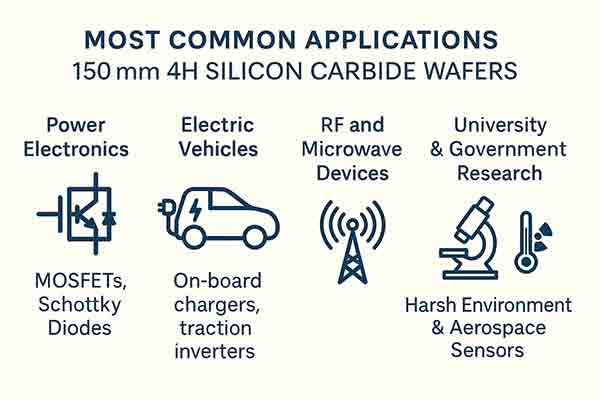
Common Applications for 150mm 4H Silicon Carbide Wafers
| Application Area | Typical Devices | Benefits of 4H-SiC |
|---|---|---|
| Power Electronics | MOSFETs, Schottky Diodes, JFETs | Lower switching losses and higher voltages |
| Electric Vehicles | Traction inverters, DC-DC converters, onboard chargers | Greater efficiency and faster charging |
| RF and Microwave Devices | 5G infrastructure, radar systems, satellite communications | High-frequency operation and thermal stability |
| Research and Development | Wide-bandgap devices, quantum materials, prototype devices | Supports advanced semiconductor research |
| Aerospace and Defense | Radiation-hardened circuits, harsh environment sensors | High reliability under extreme conditions |
Power Electronics and Electric Vehicles
One of the largest markets for silicon carbide substrates is power electronics. 150mm 4H-SiC wafers are used to manufacture high-voltage MOSFETs and Schottky diodes found in solar inverters, industrial motor drives, EV traction systems, and energy storage systems. Their superior efficiency reduces heat generation and increases power density.
RF, Microwave, and 5G Applications
4H-SiC substrates are also used in RF amplifiers, microwave devices, radar systems, and next-generation 5G communication hardware. Their high-frequency performance and excellent thermal properties make them suitable for demanding telecommunications applications.
Research, Aerospace, and Harsh Environment Electronics
Universities, government laboratories, and semiconductor manufacturers use 150mm SiC wafers for wide-bandgap device development, quantum research, and advanced materials studies. Aerospace and defense industries rely on SiC for sensors and electronics capable of operating under extreme temperatures, radiation exposure, and harsh environments.
Why Choose 150mm SiC Wafers?
As semiconductor manufacturing moves toward larger wafer diameters, 150mm 4H silicon carbide wafers provide improved manufacturing efficiency and higher device yields. They are becoming the preferred substrate for power semiconductors, electric vehicles, renewable energy systems, RF electronics, and next-generation high-performance devices.
Related Pages
- Silicon Carbide (SiC) Wafers
- Silicon Carbide Substrates
- MOSFET Substrates
- Wide Bandgap Semiconductors